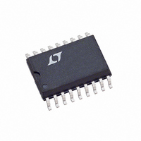
LTC1040CSW Linear Technology, LTC1040CSW Datasheet

LTC1040CSW
Specifications of LTC1040CSW
Available stocks
Related parts for LTC1040CSW
LTC1040CSW Summary of contents
Page 1
... The output of the comparator will be high if the algebraic sum of the inputs is positive and low if the algebraic sum of the inputs is negative. , LTC and LT are registered trademarks of Linear Technology Corporation. LTCMOS™ trademark of Linear Technology Corporation. Typical LTC1040 Supply Current vs Sampling Frequency ...
Page 2
... V Off LTC1040C P-P LTC1040M + V = 4.75V – 360 A OUT + V = 4.75V 1.6mA OUT U W TOP VIEW ORDER PART + NUMBER P-P LTC1040CN 16 OSC LTC1040CSW 15 B OUT + 14 B1 – – – PACKAGE 18-LEAD PLASTIC SO WIDE = 120 C/W ( C/W (SW) JA LTC1040MJ LTC1040CJ = 80 C/W JA OBSOLETE PACKAGE – ...
Page 3
ELECTRICAL CHARACTERISTICS temperature range otherwise specifications are at T SYMBOL PARAMETER STROBE Input (Note 7) V Logic “1” Input Voltage IH V Logic “0” Input Voltage IL R External Timing Resistor EXT f Sampling Frequency S Note 1: Absolute Maximum ...
Page 4
LTC1040 W U TYPICAL PERFOR A CE CHARACTERISTICS Response Time vs Temperature 130 + 120 110 100 –50 – 125 50 75 100 AMBIENT TEMPERATURE ...
Page 5
U U APPLICATIO S I FOR ATIO The LTC1040 uses sampled data techniques to achieve its unique characteristics. Some of the experience acquired using classic linear comparators does not apply to this circuit brief description of internal operation ...
Page 6
LTC1040 U U APPLICATIO S I FOR ATIO Minimizing Comparison Errors The two differential input voltages, V1 and V2, are con- verted to charge by the input capacitors C Figure 2). The charge is summed at the virtual ground point; ...
Page 7
U U APPLICATIO S I FOR ATIO Offset Voltage Error The errors due to offset, common mode, power supply variation, gain and temperature are all included in the offset voltage specification. This makes it easy to compute the error when ...
Page 8
LTC1040 U U APPLICATIO S I FOR ATIO Output Logic In addition to the normal outputs (A additional outputs and ON/0FF, are provided (see Figure 8 and Table 1). All logic is powered from V ground, thus ...
Page 9
U TYPICAL APPLICATIO S † THERMISTOR # 44007 YELLOW SPRINGS INSTRUMENT CO., INC. 82k * HYSTERESIS = 5V • = 20mV 20M 28 C SEPARATION 27 C HEAT COOL Window Comparator with Independent Window Limits and Fully Floating Differential Input ...
Page 10
LTC1040 U TYPICAL APPLICATIO S The LTC1040 as a Linear Amplifier With a simple RC filter, the LTC1040 can be made to function as a linear amplifier. By filtering the logic output and feeding it back to the negative input, ...
Page 11
... MOLD FLASH OR PROTRUSIONS SHALL NOT EXCEED .010 INCH (0.254mm) Information furnished by Linear Technology Corporation is believed to be accurate and reliable. However, no responsibility is assumed for its use. Linear Technology Corporation makes no represen- tation that the interconnection of its circuits as described herein will not infringe on existing patent rights. ...
Page 12
... LTC1040 • TA11 .447 – .463 NOTE .394 – .419 (10.007 – 10.643) N .037 – .045 (0.940 – 1.143) .004 – .012 (0.102 – 0.305) S18 (WIDE) 0502 LW/TP 1202 1K REV A • PRINTED IN USA LINEAR TECHNOLOGY CORPORATION 1991 f OUT f IN 1040fa ...


