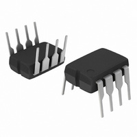
LM311NG ON Semiconductor, LM311NG Datasheet - Page 6

LM311NG
Manufacturer Part Number
LM311NG
Description
IC COMPARATOR SGL HI VOLT 8DIP
Manufacturer
ON Semiconductor
Type
General Purposer
Specifications of LM311NG
Number Of Elements
1
Output Type
DTL, MOS, Open-Collector, Open-Emitter, RTL, TTL
Voltage - Supply
5 V ~ 30 V, ±2.5 V ~ 15 V
Mounting Type
Through Hole
Package / Case
8-DIP (0.300", 7.62mm)
Number Of Channels
1 Channel
Response Time
200 ns
Offset Voltage (max)
7.5 mV
Input Bias Current (max)
100 nA
Supply Voltage (max)
36 V
Supply Voltage (min)
5 V
Supply Current (max)
2.4 mA
Maximum Power Dissipation
625 mW
Maximum Operating Temperature
+ 70 C
Mounting Style
Through Hole
Minimum Operating Temperature
0 C
Amplifier Type
Comparator
Current, Input Bias
45 nA
Current, Input Offset
1.7 nA
Current, Supply
-5 to +7.5 mA
Number Of Amplifiers
Single
Package Type
PDIP-8
Power Dissipation
625 mW
Temperature, Operating, Range
0 to +70 °C
Voltage, Gain
200 V/mV
Voltage, Input
±15 VDC
Voltage, Input Offset
2 mV
Voltage, Supply
5 to 30 V
Number Of Elements
1
Technology
Bipolar
Input Offset Voltage
7.5@±15VmV
Input Bias Current (typ)
250nA
Single Supply Voltage (typ)
9/12/15/18/24/28V
Dual Supply Voltage (typ)
±3/±5/±9/±12V
Power Supply Requirement
Single/Dual
Voltage Gain In Db
106.02dB
Single Supply Voltage (min)
5V
Single Supply Voltage (max)
30V
Dual Supply Voltage (min)
±2.5V
Dual Supply Voltage (max)
±15V
Operating Temp Range
0C to 70C
Operating Temperature Classification
Commercial
Mounting
Through Hole
Pin Count
8
Comparator Type
General Purpose
No. Of Comparators
1
Ic Output Type
DTL, MOS, RTL, TTL
Supply Current
2.4mA
Supply Voltage Range
5V To 30V
Amplifier Case Style
DIP
Rohs Compliant
Yes
Lead Free Status / RoHS Status
Lead free / RoHS Compliant
Other names
LM311NGOS
Available stocks
Company
Part Number
Manufacturer
Quantity
Price
Company:
Part Number:
LM311NG
Manufacturer:
ON Semiconductor
Quantity:
3 650
Part Number:
LM311NG
Manufacturer:
ON/安森美
Quantity:
20 000
Input
Input
Balance
Adjust
Balance
Figure 18. Zero−Crossing Detector
Figure 16. Improved Method of Adding
Hysteresis Without Applying Positive
Inputs
0.1 mF
R1
R2
V
Driving CMOS Logic
EE
C2
5.0 k
Feedback to the Inputs
+
LM311
= −15 V
3.0 k
V
V
EE
2
3
CC
−15 V
+
−
= +15 V
8
LM311
V
6
GND
CC
4
0.002
mF
5.0 k
C1
3.0 k
10 k
1
5
3.0
2.6
2.2
1.8
1.4
1.0
33 k
0.1 mF
−55
7
Output
to CMOS Logic
Postive Supply − Output Low
Positive and Negative Supply − Output High
4.7 k
82
APPLICATIONS INFORMATION
−25
Figure 15. Power Supply Current
+15 V
Output
http://onsemi.com
LM211, LM311
0
versus Temperature
T
A
, TEMPERATURE (°C)
25
6
50
Inputs
Input
Figure 19. Relay Driver with Strobe Capability
75
V
V
GND
V
V
Figure 17. Conventional Technique
EE
EE
100
CC
EE
100
R1
R2
0.1 mF
C2
+
LM311
= −15 V
= +15 V
100
for Adding Hysteresis
1.0 M
Q1
−15 V
3
2
V
V
1.0 k
Output
CC1
CC
Balance/Strobe
+
Strobe
125
−
TTL
8
LM311
2N2222 or
Equivalent
510 k
6
4
5.0 k
C1
3.0 k
V
CC2
1
5
0.1 mF
7
*Zener Diode D1
protects the comparator
from inductive kickback
and voltage transients
on the V
*D1
4.7 k
CC2
supply line.
+15 V
Output


