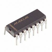
MAX912CPE+ Maxim Integrated Products, MAX912CPE+ Datasheet - Page 2

MAX912CPE+
Manufacturer Part Number
MAX912CPE+
Description
IC COMPARATOR LP 16-DIP
Manufacturer
Maxim Integrated Products
Type
with Latchr
Datasheet
1.MAX913CSA.pdf
(11 pages)
Specifications of MAX912CPE+
Number Of Elements
2
Output Type
Complementary, TTL
Mounting Type
Through Hole
Package / Case
16-DIP (0.300", 7.62mm)
Number Of Channels
2 Channels
Product
Digital Comparators
Offset Voltage (max)
3 mV
Input Bias Current (max)
8 uA
Supply Voltage (max)
10 V
Supply Voltage (min)
5 V
Supply Current (max)
10000 uA
Maximum Power Dissipation
727 mW
Maximum Operating Temperature
+ 70 C
Mounting Style
Through Hole
Minimum Operating Temperature
0 C
Lead Free Status / RoHS Status
Lead free / RoHS Compliant
ABSOLUTE MAXIMUM RATINGS
Positive Supply Voltage .........................................................+7V
Negative Supply Voltage ........................................................-7V
V+ to V- ................................................................................+13V
Differential Input Voltage .....................................................+15V
Input Voltage (Referred to V-) ................................-0.3V to +14V
Latch Pin Voltage .............................................Equal to Supplies
Continuous Output Current...............................................±20mA
Continuous Power Dissipation (T
Single/Dual, Ultra-Fast, Low-Power
Precision TTL Comparators
Stresses beyond those listed under “Absolute Maximum Ratings” may cause permanent damage to the device. These are stress ratings only, and functional
operation of the device at these or any other conditions beyond those indicated in the operational sections of the specifications is not implied. Exposure to
absolute maximum rating conditions for extended periods may affect device reliability.
ELECTRICAL CHARACTERISTICS
V+ = +5V, V- = -5V, V
2
Input Offset Voltage (Note 2)
Offset Drift
Input Offset Current (Note 2)
Input Bias Current
Input Voltage Range
Common-Mode Rejection Ratio
Power-Supply Rejection Ratio
Small-Signal Voltage Gain
Output Voltage
Positive Supply Current Per
Comparator (Note 3)
Negative Supply Current Per
Comparator (Note 3)
Latch-Pin High Input Voltage
Latch-Pin Low Input Voltage
Latch-Pin Current
8-Pin Plastic DIP (derate 9.09mW/°C above +70°C) ...727mW
_______________________________________________________________________________________
PARAMETER
Q
= 1.4V, V
A
LE
= +70°C)
= 0V, T
SYMBOL
TCV
CMRR
PSRR
V
V
V
V
I
V
V
A
OS
I+
I
I
OS
CM
OH
I-
OL
IL
B
IH
IL
V
OS
A
= T
MIN
R
T
T
T
C, E temperature ranges
C, E temperature ranges
Single +5V
-5.0V
Positive supply; 4.5V
Negative supply; -2V
1V
V+
I
T
C, E temperature ranges
V
SINK
A
A
A
A
LE
S
to T
= +25°C
= T
= +25°C
= +25°C, I
= 0V
100
V
4.5V
= 4mA
Q
MIN TO
MAX
V
CM
2V, T
, unless otherwise noted. Typical values are at T
T
SINK
+3.5V
MAX
CONDITIONS
A
= +25°C
= 10mA
T
T
C, E temperature ranges
I
I
OUT
OUT
Operating Temperature Ranges:
MAX91_C_ _ ...........................................................0°C to +70°C
MAX91_E_ _.........................................................-40°C to +85°C
Storage Temperature Range .............................-65°C to +150°C
Lead Temperature (soldering, 10s) .................................+300°C
A
A
= +25°C
= T
8-Pin SO (derate 5.88mW/°C above +70°C)................471mW
8-Pin µMAX (derate 4.5mW/°C above +70°C) .............362mW
16-Pin Plastic DIP (derate 10.53mW/°C above +70°C)842mW
16-Pin Narrow SO (derate 8.70mW/°C above +70°C) .696mW
V+
V-
= 1mA
= 10mA
MIN TO
-7V
5.5V
T
MAX
1500
MIN
-5.2
-0.2
2.7
2.4
2.0
80
60
80
3500
TYP
110
100
0.1
0.3
3.4
3.0
0.3
0.4
85
-1
A
2
2
6
1
= +25°C.) (Note 1)
MAX
+3.5
+3.5
0.5
0.5
0.8
-20
10
2
3
1
5
8
2
UNITS
µV/°C
mV
V/V
mA
mA
dB
dB
µA
µA
µA
V
V
V
V


