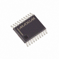
MAX9601EUP+ Maxim Integrated Products, MAX9601EUP+ Datasheet - Page 10

MAX9601EUP+
Manufacturer Part Number
MAX9601EUP+
Description
IC COMPARATOR HS 20-TSSOP
Manufacturer
Maxim Integrated Products
Type
General Purposer
Datasheet
1.MAX9600EUP.pdf
(12 pages)
Specifications of MAX9601EUP+
Number Of Elements
2
Output Type
Complementary, Differential, PECL
Mounting Type
Surface Mount
Package / Case
20-TSSOP
Number Of Channels
2 Channels
Supply Voltage (max)
6.3 V
Supply Voltage (min)
4.3 V
Supply Current (max)
27 mA
Maximum Operating Temperature
+ 85 C
Mounting Style
SMD/SMT
Minimum Operating Temperature
- 40 C
Propagation Delay Time
500 ps
Comparator Type
High Speed
No. Of Comparators
2
Response Time
500ps
Ic Output Type
Differential, PECL
Supply Current
19mA
Supply Voltage Range
4.3V To 6.3V, -4V To -6V
Rohs Compliant
Yes
Lead Free Status / RoHS Status
Lead free / RoHS Compliant
The MAX9600/MAX9601 incorporate latch-enable and
hysteresis control. Hysteresis rejects noise and pre-
vents oscillations on low-slew input signals. The latch-
enable control permits tracking or sampling mode of
operations. Drive the complementary latch enable with
standard ECL logic for MAX9600 and PECL logic for
MAX9601. The MAX9602 quad-channel PECL output
comparator does not include the latch-enable or hys-
teresis control functions.
Special layout precautions exist due to the large gain-
bandwidth characteristic of the MAX9600/MAX9601/
MAX9602. Use a printed circuit board with a good, low-
inductance ground plane. Mount 0.01µF ceramic
decoupling capacitors as close to the power-supply
inputs as possible. Minimize lead lengths on the inputs
and outputs to avoid unwanted parasitic feedback
around the comparators. Use surface-mount chip com-
ponents to minimize lead inductance. Pay close atten-
tion to the bandwidth of the decoupling and terminating
components.
Use microstrip layout and terminations at the input and
output. Avoid discontinuities in differential impedance.
Maximize common-mode noise immunity by maintain-
ing the distance between differential traces and avoid
sharp corners. Minimize the number of vias to prevent
impedance discontinuities. Match the electrical length
of the traces to minimize skew.
As with all high-speed comparators, the high gain-
bandwidth product of these devices can create oscilla-
tion problems when the input goes through the
threshold region. This is typically due to parasitic paths,
which cause positive feedback to occur. For clean
switching without oscillation or steps in the output
waveform for the MAX9600/MAX9601, use an input with
a slew rate of 5V/µs or faster. For the MAX9602, use a
slew rate of 25V/µs or faster. The tendency of the part
to oscillate is a function of the layout and source imped-
ance of the circuit employed. Poor layout and larger
source impedance increases the minimum slew-rate
requirement. Adding hysteresis accommodates slower
inputs (see the Hysteresis section).
Hysteresis can be introduced to prevent oscillation or
multiple transitions due to noise. The MAX9600/
MAX9601 feature current-controlled hysteresis, which is
set by placing a resistor between HYS_ and GND. The
value of the current-setting resistor is determined by the
Dual ECL and Dual/Quad PECL, 500ps,
Ultra-High-Speed Comparators
10
______________________________________________________________________________________
Applications Information
Input Slew-Rate Requirements
Hysteresis (MAX9600/MAX9601)
Layout
output voltage of 2.5V at HYS_ divided by the desired
hysteresis current level in the range of 0 to 200µA.
R
60mV to 5mV (see the Hysteresis vs. R
graph in the Typical Operating Characteristics section).
For a zero hysteresis (0µA hysteresis current), leave
HYS_ open or connect it to V
Propagation delay dispersion is defined as a variation
in propagation delay as a function of change in input
conditions. In an automatic test system pin-driver elec-
tronics, for example, the dispersion determines the
maximum edge resolution.
Many factors can affect the dispersion, such as common-
mode voltage, overdrive, input slew rate, duty cycle, and
pulse width. The typical propagation delay dispersions of
the MAX9600/MAX9601/MAX9602 are less than 10ps to
40ps (see the Typical Operating Characteristics and
Electrical Characteristics sections).
The latch-enable function allows the comparator to be
used in a sampling mode. When LE_ is low (LE_ is high),
the comparator tracks the input signal. When LE_ is dri-
ven high (LE_ is low), the outputs are forced to an unam-
biguous logic state, dependent on the input conditions at
the time of the latch input transition. If the latch-enable
function is not used, connect the appropriate LE_ input
to a low ECL/PECL logic, and its complementary LE_
input to a high ECL/PECL logic level (see Table 1).
The input range of the MAX9600 differential latch-
enable inputs is 400mV to 2V. The logic-input swing
excursion must fall within an input-voltage range (V
of -2V to 0 to work properly. The input range of the
MAX9601 differential latch-enable inputs is 250mV to
3.5V. The logic-input swing excursion must fall within an
input-voltage range (V
3.5V) or V
3.5V) to work properly.
Table 1. Latch-Enable Truth Table
HYS
LATCH-ENABLE INPUT
LE_
0
1
0
1
of 10kΩ to 35kΩ resistors provides hysteresis of
LR
of (V
Comparators with Latch Enable
LE
Propagation Delay Dispersion
1
0
0
1
CCO
_ _ _ _
_ - 3.5V) to V
LR
Compare Mode. Output follows
input state.
Latch Mode. Output latches to
last known output state.
Invalid condition, output is in
unknown state.
) of 0 to 3.5V for (V
CC
(MAX9600/MAX9601)
.
OPERATION
CCO
_ for (V
HYS
to GND
CCO
CCO
_ <
LR
_ ≥
)


