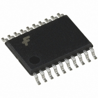
FMS6346MTC20X Fairchild Semiconductor, FMS6346MTC20X Datasheet - Page 7

FMS6346MTC20X
Manufacturer Part Number
FMS6346MTC20X
Description
IC DRIVER VIDEO FLTR 6CH 20TSSOP
Manufacturer
Fairchild Semiconductor
Type
Driverr
Datasheet
1.FMS6346MTC20X.pdf
(10 pages)
Specifications of FMS6346MTC20X
Applications
Recorders, Set-Top Boxes
Mounting Type
Surface Mount
Package / Case
20-TSSOP
Frequency
74.25MHz
Bandwidth
34MHz
Attenuation
41dB
Filter Order
6th
Supply Voltage Range
4.75V To 5.25V
Tv / Video Case Style
TSSOP
No. Of Pins
20
Termination Type
SMD
Rohs Compliant
Yes
Filter Terminals
SMD
Digital Ic Case Style
TSSOP
Lead Free Status / RoHS Status
Lead free / RoHS Compliant
Other names
FMS6346MTC20XTR
FMS6346MTC20X_NL
FMS6346MTC20X_NLTR
FMS6346MTC20X_NLTR
FMS6346MTC20X_NL
FMS6346MTC20X_NLTR
FMS6346MTC20X_NLTR
Available stocks
Company
Part Number
Manufacturer
Quantity
Price
Part Number:
FMS6346MTC20X
Manufacturer:
FAIRCHILD/ن»™ç«¥
Quantity:
20 000
© 2006 Fairchild Semiconductor
FMS6346 • Rev. 1.0.5
The same method can be used for biased signals with the
addi tion of a pull-up resistor to make sure the clamp never
operates. The internal pull-down resistance is 800kΩ
±20%, so the exter nal resistance should be 7.5MΩ to set
the DC level to 500mV. If a pull-up resistance less than
7.5MΩ is desired, an external pull-down can be added
such that the DC input level is set to 500mV.
The same circuits can be used with AC-coupled outputs if
desired, as shown in Figure 17.
NOTE: The video tilt or line time distortion is dominated by
the AC-coupling capacitor. The value may need to be in-
creased beyond 220μF to obtain satisfactory operation in
some applications.
Figure 16. Biased SCART with DC-Coupled Outputs
Figure 18. AC-Coupled Inputs, AC-Coupled Outputs
Figure 19. Biased SCART with AC-Coupled Outputs
External video
source must
be AC coupled
Figure 17 DC-Coupled Inputs, AC-Coupled Outputs
External video
source must
be AC coupled.
DVD or
Output
DVD or
Output
DAC
STB
SoC
DAC
STB
SoC
75Ω
75Ω
500mV +/-350mV
0V - 1.4V
0.1μF
0.1μF
500mV +/-350mV
7.5MΩ
0.1μF
7.5MΩ
0V - 1.4V
Inactive
Clamp
LCVF
Clamp
Active
LCVF
Clamp
Active
LCVF
LCVF
Input
Bias
75Ω
75Ω
75Ω
220µF
75Ω
220μF
220μF
7
Power Dissipation
The FMS6346 output drive confi guration must be consid-
ered when calculating overall power dissipation. Care
must be taken not to exceed the maximum die junction
temperature. The fol lowing example can be used to calcu-
late the FMS6346’s power dissipation and internal tem-
perature rise:
where P
and P
where
V
I
V
I
V
R
Board layout can affect thermal characteristics. Refer to
the Layout Considerations section for more information.
Layout Considerations
General layout and supply bypassing play major roles in
high-frequency performance and thermal characteristics.
Fairchild offers a demonstration board, FMS6346DEMO,
to guide layout and aid device testing and characteriza-
tion. The FMS6346DEMO is a four-layer board with a full
power and ground plane. Following this layout confi gura-
tion pro vides the optimum performance and thermal char-
acteristics. For best results, follow the steps below as a
basis for high-fre quency layout:
• Include 10μF and 0.1μF ceramic bypass capacitors
• Place the 10μF capacitor within 0.75 inches of the
• Place the 0.1μF capacitor within 0.1 inches of the
• For multi-layer boards, use a large ground plane to
• For two-layer boards, use a ground plane that extends
• Minimize all trace lengths to reduce series inductances
Output Considerations
The FMS6346 outputs are DC offset from the input by
150mV. Therefore, V
required to obtain optimal performance from the output
driver and is held at the minimum value to decrease the
standing DC current into the load. Since the FMS6346
has a 2x (6dB) gain, the output is typically connected via a
75Ω-series back-matching resistor, followed by the 75Ω
video cable. Due to the inherent divide by two of this confi -
guration, the blanking level at the load of the video signal
is always less than 1V. When AC-coupling the output,
ensure that the coupling capacitor of choice passes the
lowest frequency content in the video signal and that line
time distortion (video tilt) is kept as low as possible.
T
CH
CC
O
IN
s
L
J
power pin
power pin
help dissi pate heat
beyond the device by at least 0.5 inches
= 5V
= channel load resistance
= T
= 2V
= (I
= 60mA
= RMS value of input signal
CHx
A
CC
+ P
in
d
/ 6) + (V
= V
+ 0.280V
= P
d
• θ
s
CH1
• I
JA
CH
+ P
O
- (V
/R
CH2
L
OUT
O
)
2
+ P
/R
= 2•V
L
CHx
)
IN
DC+150mV. This offset is
www.fairchildsemi.com


