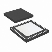
DS16EV5110ASQE/NOPB National Semiconductor, DS16EV5110ASQE/NOPB Datasheet - Page 10

DS16EV5110ASQE/NOPB
Manufacturer Part Number
DS16EV5110ASQE/NOPB
Description
IC EQUALIZER VIDEO 3D+C 48LLP
Manufacturer
National Semiconductor
Type
Video Equalizerr
Datasheet
1.DS16EV5110ASQXNOPB.pdf
(20 pages)
Specifications of DS16EV5110ASQE/NOPB
Applications
HD Displays, DVI/HDMI
Mounting Type
Surface Mount
Package / Case
48-LLP
Supply Voltage Range
3V To 3.6V
Operating Temperature Range
-40°C To +85°C
Digital Ic Case Style
LLP
No. Of Pins
48
Msl
MSL 3 - 168 Hours
Filter Terminals
SMD
No. Of I/o's
8
Rohs Compliant
Yes
Communication Function
Multi-Channel Equalizer
Lead Free Status / RoHS Status
Lead free / RoHS Compliant
Other names
DS16EV5110ASQETR
Available stocks
Company
Part Number
Manufacturer
Quantity
Price
www.national.com
DS16EV5110A Device Description
The DS16EV5110A video equalizer comprises three data
channels, a clock channel, and a control interface including a
Systeml Management Bus (SMBus) port.
DATA CHANNELS
The DS16EV5110A provides three data channels. Each data
channel consists of an equalizer stage, a limiting amplifier, a
DC offset correction block, and a TMDS driver as shown in
Figure 3.
EQUALIZER BOOST CONTROL
The data channel equalizers support eight programmable lev-
els of equalization boost. The state of the FEB pin determines
how the boost settings are controlled. If the FEB pin is held
High, then the equalizer boost setting is controlled by the
Boost Set pins (BST_[0:2]) in accordance with Table 2. If this
programming method is chosen, then the boost setting se-
lected on the Boost Set pins is applied to all three data
channels. When the FEB pin is held Low, the equalizer boost
level is controlled through the SMBus. This programming
method is accessed via the appropriate SMBus registers (see
Table 1). Using this approach, equalizer boost settings can
be programmed for each channel individually. FEB is inter-
nally pulled High (default setting); therefore if left unconnect-
ed, the boost settings are controlled by the Boost Set pins
(BST_[0:2]). The range of boost settings provided enables the
DS16EV5110A to address a wide range of transmission line
path loss scenarios, enabling support for a variety of data
rates and formats.
DEVICE STATE AND ENABLE CONTROL
The DS16EV5110A has an Enable feature which provides the
ability to control device power consumption. This feature can
BC_2, BC_1,
Control Via
(FEB = 0)
SMBus
BC_0
000
001
010
011
100
101
110
111
TABLE 2. EQ Boost Control Table
Control Via Pins
BST_2, BST_1,
(FEB = 1)
BST_0
000
001
010
011
100
101
110
111
EQ Boost Setting
at 825 MHz (dB)
(TYP)
14
18
21
24
26
28
30
9
10
be controlled either via the Enable Pin (EN Pin) or via the
Enable Control Bit which is accessed through the SMBus port
(see Table 1 and Table 3). If Enable is activated, the data
channels and clock channel are placed in the ACTIVE state
and
DS16EV5110A can also be placed in STANDBY mode to
save power. In this mode only the control interface including
the SMBus port as well as the clock channel signal detection
circuit remain active.
CLOCK CHANNEL
The clock channel incorporates a limiting amplifier, a DC off-
set correction, and a TMDS driver as shown in Figure 4.
CLOCK CHANNEL SIGNAL DETECT
The DS16EV5110A features a signal detect circuit on the
clock channel. The status of the clock signal can be deter-
mined by either reading the Signal Detect bit (SD) in the
SMBus registers (see Table 1) or by the state of the SD pin.
A logic High indicates the presence of a signal that has ex-
ceeded a specified threshold value (called SD_ON). A logic
Low means that the clock signal has fallen below a threshold
value (called SD_OFF). These values are programmed via
the SMBus (Table 1). If not programmed via the SMBus, the
thresholds take on the default values for the SD_OFF and
SD_ON values as indicated in Table 4. The Signal Detect
threshold values can be changed through the SMBus. All
threshold values specified are DC peak-to-peak differential
signals (positive signal minus negative signal) at the input of
the device.
TABLE 4. Clock Channel Signal Detect Threshold Values
Register 07[0]
Bit 1 Bit 0
0
0
1
1
0 : Disable
0 : Disable
1 : Enable
1 : Enable
(SMBus)
all
TABLE 3. Enable and Device State Control
0
1
0
1
device
SD_OFF Threshold
Register 06 (mV)
(CMOS)
EN Pin
blocks
40 (Default)
X
X
1
0
30
55
45
function
Register 03[3]
(EN Control)
(SMBus)
X
X
0
1
as
SD_ON Threshold
Register 05 (mV)
70 (Default)
described.
Device State
STANDBY
STANDBY
55
90
75
ACTIVE
ACTIVE
The


