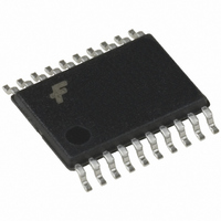
FMS6403MTC20 Fairchild Semiconductor, FMS6403MTC20 Datasheet - Page 12

FMS6403MTC20
Manufacturer Part Number
FMS6403MTC20
Description
IC DRIVER VID TRPL FLTR 20TSSOP
Manufacturer
Fairchild Semiconductor
Type
Driverr
Datasheet
1.FMS6403MTC20X.pdf
(14 pages)
Specifications of FMS6403MTC20
Applications
Recorders, Set-Top Boxes
Mounting Type
Surface Mount
Package / Case
20-TSSOP
Lead Free Status / RoHS Status
Lead free / RoHS Compliant
Other names
FMS6403MTC20_NL
FMS6403MTC20_NL
FMS6403MTC20_NL
Available stocks
Company
Part Number
Manufacturer
Quantity
Price
Company:
Part Number:
FMS6403MTC20X
Manufacturer:
FAIRCHILD
Quantity:
192
Part Number:
FMS6403MTC20X
Manufacturer:
FAIRCHILD/ن»™ç«¥
Quantity:
20 000
© 2005 Fairchild Semiconductor Corporation
FMS6403 • Rev. 1.0.4
Applications Information
Input Circuitry
The DC restore circuit requires a source impedance
(R
correct operation. Driving the FMS6403 with a high-
impedance source (e.g. a DAC loaded with 330Ω) does
not yield optimum results. Refer Figure 2 for details.
Output Drive
The FMS6403 is specified to operate with output
currents typically less than 60mA, more than sufficient
for a dual (75Ω) video load. Internal amplifiers are
current limited to approximately 100mA and should
withstand
however, this capability is not guaranteed.
The maximum specified input voltage of 1.5V
sustained for all inputs. When the input is clamped to
1.125V, this does not result in a meaningful output
signal. With a gain of 6dB, the output should be 1.125V
±1.5V, which is not possible since the output cannot
drive below ground. This condition will not damage the
part; however, the output will be clipped. For signals
clamped to 250mV, this does not occur.
Signals at mid-scale during SYNC (Pb and Pr) must be
clamped to 1.125V. Signals that are at their lowest
during SYNC (Y, R, G, B) must be clamped to 250mV
for proper operation. Clamping a Pr signal to 250mV
results in clipping the bottom of the signal.
The
termination, as shown in the Figure 2, forms a high-
pass filter that blocks the DC while passing the video
frequencies and avoiding tilt. Any value lower than
220μF creates problems, such as video tilt. Higher
values, such as 470μF - 1000μF, are the most optimal
output coupling capacitor. By AC coupling, the average
DC level is zero and the output voltages of all channels
is centered ~zero.
Sync Recovery
The FMS6403 typically recovers bi-level sync with
amplitude greater than 100mV (33% compressed
relative to the nominal 300mV amplitude). The
FMS6403 looks for the lowest signal voltage and
clamps this to approximately 250mV at the output.
Tri-level sync may not be compressed more than 5%
(15mV) for correct operation. Tri-level sync is located by
finding the edges of the tri-level pulse and running a
timer to operate the clamp during the back porch
interval.
The selection of the 8MHz or 15MHz filters enables bi-
level sync recovery. Selection of the 30MHz filter or
bypass mode enables tri-level sync recovery. Bi-level
and tri-level sync recovery are not interchangeable. See
the Sync Processing section for more information.
P
The output drive configuration must be considered
when calculating overall power dissipation. Care must
be taken not to exceed the maximum die junction
temperature. The following example can be used to
ower Dissipation
SOURCE
220µF
= R
brief-duration,
S
|| R
capacitor
T
) of less than or equal to 150Ω for
coupled
short-circuit
with
the
conditions;
PP
can be
150Ω
12
calculate the FMS6403’s power dissipation and internal
temperature rise:
T
where:
P
and:
PCHx = V
where:
V
I
V
I
V
R
Board layout can also affect thermal characteristics.
Refer to the Layout Considerations Section for more
information. The FMS6403 is specified to operate with
output currents typically less than 60mA, more than
sufficient for a single (150Ω) video load. Internal
amplifiers are current limited to a maximum of 100mA
and should withstand brief duration short circuit
conditions, however this capability is not guaranteed.
Layout Considerations
General layout and supply bypassing play major roles in
high-frequency
characteristics. Fairchild offers an evaluation board,
FMS6403DEMO, to guide layout and aid device testing
and characterization. The FMS6403DEMO is a four-
layer board with a full power and ground planes. For
optimum results, follow the steps below as a basis for
high-frequency layout:
If using multiple, low-impedance DC-coupled outputs;
special layout techniques can help dissipate heat. For
dual-layer boards, place a 0.5-inch to 1-inch (1.27cm to
2.54cm) square ground plane directly under the device
and on the bottom side of the board. Use multiple vias
to connect the ground planes. For multi-layer boards,
additional planes (connected with vias) can be used for
additional thermal improvements.
Worst-case additional die power due to DC loading can
be estimated at (V
assumes a constant DC output voltage of V
V
per channel.
CH
CC
J
D
O
IN
S
CC
L
= T
= P
= 5V
= channel load resistance
= 2V
= (I
= 90mA
= RMS value of input signal
with a dual DC video load, add 25/(4•75) = 83mW,
Include 10μF and 0.1μF ceramic bypass
capacitors.
Place the 10μF capacitor within 0.75 inches of the
power pin.
Place the 0.1μF capacitor within 0.1 inches of the
power pin.
Connect all external ground pins as tightly as
possible, preferably with a large ground plane
under the package.
Layout channel connections to reduce mutual trace
inductance.
Minimize all trace lengths to reduce series
inductances. If routing across a board, place devise
such that longer traces are at the inputs rather than
the outputs.
A
CH1
CC
+ Pd Θ
IN
/ 3) + (V
+ P
S
+ 0.280V
• I
CH2
CH
JA
- (V
+ P
O
CC
/R
O
CH3
2
2
performance
L
/4R
/R
)
L
)
load
) per output channel. This
and
CC
www.fairchildsemi.com
2
. For 5V
thermal
(1)


