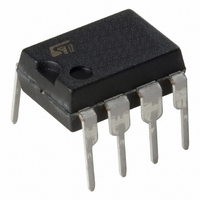
TEA2031A STMicroelectronics, TEA2031A Datasheet - Page 3

TEA2031A
Manufacturer Part Number
TEA2031A
Description
IC CORRECTION EAST/WEST 8-PDIP
Manufacturer
STMicroelectronics
Type
Videor
Datasheet
1.TEA2031A.pdf
(11 pages)
Specifications of TEA2031A
Applications
Displays, Monitors, TV
Mounting Type
Through Hole
Package / Case
8-DIP (0.300", 7.62mm)
Lead Free Status / RoHS Status
Lead free / RoHS Compliant
Available stocks
Company
Part Number
Manufacturer
Quantity
Price
Company:
Part Number:
TEA2031A
Manufacturer:
OMRON
Quantity:
5 510
Part Number:
TEA2031A
Manufacturer:
ST
Quantity:
20 000
the required current via a series resistor to pin 1.
Likewise, the current to pin 2 is drawn through a
series resistor from an external dc voltage source.
These series resistors can have values of around
40kΩ resulting in input currents of approximately
0.1mA ± modulation current.
Pin 7 should be loaded to ground through a 100kΩ
resistor which as a result will produce a parabola
of 5 volts peak-to-peak at pin 7. This parabola is
symmetrical if the DC current flowing into pin 2 is
equal to the mean input current of pin 1. Other-
wise, the parabola becomes dissymmetrical and
produces a keystone effect correction.
The line saw-tooth at pin 8 is obtained by feeding
the line fly-back voltage through an integrator net-
Table 1. Absolute Maximum Ratings
Table 2. Thermal Data
(T
Table 3. ELECTRICAL OPERATING CHARACTERISTICS
amb
Symbol
I
1
Symbol
I
Symbol
V
V
1
R
mean
I
1PP
∆I
P
T
= + 50°C)
V
6–4
I
3–4
I
and I
I
I
I
I
th (j-a)
6
2
5–4
5–6
STG
5–4
5–6
TOT
2
6–4
2
Supply Voltage
Supply Current (R
No Load Consumption (R
Voltage Reference (R
Frame Saw-tooth Input DC Mean Current
R1 = 39kΩ at 2.5V Mean - saw-tooth Voltage
Frame Saw-tooth Input Peak-to-peak Current
R1 = 39kΩ at 2.5V Mean - saw-tooth Voltage
Keystone Correction Input DC Current
If I
Keystone Correction Input DC Current for Maximum Keystone Effect
1
Supply Voltage
Output Sink Current
Diode Output Current
Input Current
Power Dissipation
Storage Temperature Range
Non Repetitive Peak Current on Output Transistor
Non Repetitive Peak Current on Output Diode
Junction-ambient Thermal Resistance
Mean = I
2
: No Keystone Effect. R
(3-4)
(3-4)
= 22kΩ ; I
(3-4)
= 22kΩ)
Parameter
Parameter
Parameter
= 22kΩ ; I
OUT
= 0)
2
OUT
= 39kΩ at 2.5V DC ref.
= 0 ; V
work formed by a diode and a grounded capacitor
(see typical application diagram). The DC compo-
nent of the line saw-tooth is compensated by an in-
ternal current sinking source ; so that the mean DC
values of line saw-tooth and frame parabola volt-
ages are equal.
Line saw-tooth and frame parabola signals are ap-
plied to a comparator whose output is in the form
of width modulated pulses. During every pulse du-
ration, the output (pin 5) can sink external coil cur-
rents of up to 0.5A associated with diode
modulator of the main horizontal scanning circuit.
An internal recovery diode feeds back the fly-back
energy of the coil to the power supply. This diode
can carry currents of up to 0.5A.
(6-4)
= 24V)
Min.
5.9
16
– 20 to 150
Value
Value
– 0.5
0.5
0.5
0.8
1.5
1.5
35
80
± 12.5
Typ.
100
0.1
0.1
6.3
24
70
4
Max.
TEA2031A
150
6.7
35
6
°C/W
Unit
Unit
mA
°C
W
V
A
A
A
A
Unit
mW
mA
mA
mA
µA
µA
V
V
3/11


