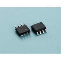
AP4563GM Advanced Power Electronics Corp., AP4563GM Datasheet
AP4563GM
Specifications of AP4563GM
Available stocks


Related parts for AP4563GM

AP4563GM Summary of contents
Page 1
... Thermal Data Symbol Rthj-a Thermal Resistance Junction-ambient Data and specifications subject to change without notice N AND P-CHANNEL ENHANCEMENT MODE POWER MOSFET SO-8 S1 N-channel Parameter 3 AP4563GM Pb Free Plating Product N-CH BV 40V DSS R 30mΩ DS(ON) I 6.7A D P-CH BV -40V DSS R 36mΩ DS(ON ...
Page 2
... AP4563GM N-CH Electrical Characteristics@T Symbol Parameter BV Drain-Source Breakdown Voltage DSS ΔBV Breakdown Voltage Temperature Coefficient /ΔT DSS j R Static Drain-Source On-Resistance DS(ON) V Gate Threshold Voltage GS(th) g Forward Transconductance fs I Drain-Source Leakage Current (T DSS Drain-Source Leakage Current (T I Gate-Source Leakage GSS Q Total Gate Charge g Q Gate-Source Charge ...
Page 3
... I =- =-30V DS V =-4. =-20V =3.3Ω, =20Ω = =-25V DS f=1.0MHz f=1.0MHz Test Conditions 2 I =-6A =-6A dI/dt=-100A/µs AP4563GM Min. Typ. Max. Units -40 - =-1mA - -0. =-250uA - ...
Page 4
... AP4563GM N-Channel Drain-to-Source Voltage (V) DS Fig 1. Typical Output Characteristics Gate-to-Source Voltage (V) GS Fig 3. On-Resistance v.s. Gate Voltage =150 0.2 0.4 0 Source-to-Drain Voltage (V) SD Fig 5. Forward Characteristic of ...
Page 5
... Fig 8. Typical Capacitance Characteristics 1 100us 0.1 1ms 10ms 0.01 100ms 1s 10s DC 0.001 10 100 0.0001 Fig 10. Effective Transient Thermal Impedance o T =150 C 4. Fig 12. Gate Charge Waveform AP4563GM f=1.0MHz Drain-to-Source Voltage (V) DS Duty factor=0.5 0.2 0.1 0.05 0.02 0. Single Pulse Duty factor = t/T Peak ...
Page 6
... AP4563GM P-Channel = Drain-to-Source Voltage (V) DS Fig 1. Typical Output Characteristics 100 Gate-to-Source Voltage (V) GS Fig 3. On-Resistance v.s. Gate Voltage =150 0.2 0.4 0.6 0 Source-to-Drain Voltage (V) SD Fig 5. Forward Characteristic of ...
Page 7
... Fig 8. Typical Capacitance Characteristics 1 100us 1ms 0.1 10ms 100ms 0. 0.001 0.0001 10 100 Fig 10. Effective Transient Thermal Impedance -4. =150 Fig 12. Gate Charge Waveform AP4563GM f=1.0MHz Drain-to-Source Voltage (V) DS Duty factor=0.5 0.2 0.1 0.05 0.02 0. Single Pulse Duty factor = t/T Peak T ...