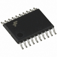
74VHC541MTC Fairchild Semiconductor, 74VHC541MTC Datasheet - Page 4

74VHC541MTC
Manufacturer Part Number
74VHC541MTC
Description
IC BUFF/DVR TRI-ST 8BIT 20TSSOP
Manufacturer
Fairchild Semiconductor
Series
74VHCr
Specifications of 74VHC541MTC
Logic Type
Buffer/Line Driver, Non-Inverting
Number Of Elements
1
Number Of Bits Per Element
8
Current - Output High, Low
8mA, 8mA
Voltage - Supply
2 V ~ 5.5 V
Operating Temperature
-40°C ~ 85°C
Mounting Type
Surface Mount
Package / Case
20-TSSOP
Logic Family
VHC
Logical Function
Buffer/Line Driver
Number Of Elements
1
Number Of Channels
8
Number Of Inputs
8
Number Of Outputs
8
Operating Supply Voltage (typ)
2.5/3.3/5V
Package Type
TSSOP W
Output Type
3-State
Polarity
Non-Inverting
Propagation Delay Time
17.5ns
High Level Output Current
-8mA
Low Level Output Current
8mA
Operating Supply Voltage (max)
5.5V
Operating Supply Voltage (min)
2V
Quiescent Current
4uA
Technology
CMOS
Pin Count
20
Mounting
Surface Mount
Operating Temp Range
-40C to 85C
Operating Temperature Classification
Industrial
Number Of Channels Per Chip
Octal
Supply Voltage (max)
5.5 V
Supply Voltage (min)
2 V
Maximum Operating Temperature
85 C
Mounting Style
SMD/SMT
Input Bias Current (max)
4 uA
Minimum Operating Temperature
- 40 C
Number Of Lines (input / Output)
8
Logic Device Type
Buffer/Line Driver, Non Inverting
Supply Voltage Range
2V To 5.5V
Logic Case Style
TSSOP
No. Of Pins
20
Operating Temperature Range
-40°C To +85°C
Filter Terminals
SMD
Rohs Compliant
Yes
Family Type
VHC
Lead Free Status / RoHS Status
Lead free / RoHS Compliant
Available stocks
Company
Part Number
Manufacturer
Quantity
Price
Part Number:
74VHC541MTCX
Manufacturer:
FAIRCHILD/ن»™ç«¥
Quantity:
20 000
©1997 Fairchild Semiconductor Corporation
74VHCT00A Rev. 1.4.0
DC Electrical Characteristics
Noise Characteristics
Note:
5. Parameter guaranteed by design.
AC Electrical Characteristics
Note:
6. C
Symbol
Symbol
t
current consumption without load. Average operating current can be obtained from the equation:
I
Symbol
V
V
V
PLH
V
CC
V
I
I
V
V
I
V
CCT
OFF
I
OLP
PD
OLV
CC
IHD
ILD
OH
IN
OL
C
IH
IL
C
(Opr.)
, t
PD
IN
is defined as the value of the internal equivalent capacitance, which is calculated from the operating
(5)
(5)
(5)
(5)
PHL
HIGH Level Input
Voltage
LOW Level Input
Voltage
HIGH Level Output
Voltage
LOW Level Output
Voltage
Input Leakage
Current
Quiescent Supply
Current
Maximum I
Output Leakage
Current (Power
Down State)
Quiet Output Maximum Dynamic V
Quiet Output Minimum Dynamic V
Minimum HIGH Level Dynamic Input Voltage
Maximum LOW Level Dynamic Input Voltage C
C
Propagation Delay
Input Capacitance
Power Dissipation
Capacitance
Parameter
PD
• V
Parameter
CC
CC
/ Input
• f
IN
Parameter
+ I
CC
V
0 – 5.5
CC
/ 4 (per gate)
4.5
5.5
4.5
5.5
4.5
4.5
5.5
5.5
0.0
(V)
V
5.0 ± 0.5
CC
V
or V
V
or V
V
V
V
Inputs
V
(V)
OUT
IN
IN
IN
IN
IN
OL
IL
IL
OL
Conditions
V
V
5.5V or GND
V
3.4V, Other
C
C
V
(6)
Conditions
IH
IH
CC
CC
5.5V
L
L
V
CC
or GND
I
I
I
I
15pF
50pF
OH
OH
OL
OL
Open
or GND
4
C
C
C
Conditions
50µA
8mA
–50µA
–8mA
L
L
L
L
50pF
50pF
50pF
50pF
Min.
Min.
4.40
3.94
2.0
2.0
T
A
T
Typ.
5.0
5.5
A
17
V
4
25°C
Typ.
CC
4.50
0.0
5.0
5.0
5.0
5.0
25°C
(V)
Max.
6.9
7.9
10
Max.
±0.1
0.36
1.35
0.8
0.8
0.1
2.0
0.5
Typ.
–0.4
0.4
T
Min.
T
1.0
1.0
A
to +85°C
A
Min.
T
4.40
3.80
2.0
2.0
to +85°C
A
25°C
–40°C
Limit
–0.8
Max.
–40°C
0.8
2.0
0.8
8.0
9.0
10
Max.
0.44
±1.0
20.0
1.50
www.fairchildsemi.com
0.8
0.8
0.1
5.0
Units
Units
Units
pF
pF
ns
V
V
V
V
mA
µA
µA
µA
V
V
V
V


