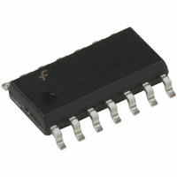
MM74C906M Fairchild Semiconductor, MM74C906M Datasheet - Page 2

MM74C906M
Manufacturer Part Number
MM74C906M
Description
IC BUFFER HEX OP/DR N-INV 14SOIC
Manufacturer
Fairchild Semiconductor
Series
74Cr
Specifications of MM74C906M
Logic Type
Buffer/Line Driver, Non-Inverting with Open Drain
Number Of Elements
6
Number Of Bits Per Element
1
Voltage - Supply
3 V ~ 15 V
Operating Temperature
-40°C ~ 85°C
Mounting Type
Surface Mount
Package / Case
14-SOIC (3.9mm Width), 14-SOL
Logic Family
74C
Number Of Channels Per Chip
Hex
Polarity
Non-Inverting
Supply Voltage (max)
15 V
Supply Voltage (min)
3 V
Maximum Operating Temperature
85 C
Mounting Style
SMD/SMT
Maximum Power Dissipation
500 mW
Minimum Operating Temperature
- 40 C
Output Type
Open Drain
Propagation Delay Time
150 ns @ 5 V or 75 ns @ 10 V
Number Of Lines (input / Output)
6 / 6
Lead Free Status / RoHS Status
Lead free / RoHS Compliant
Current - Output High, Low
-
Lead Free Status / Rohs Status
Lead free / RoHS Compliant
Available stocks
Company
Part Number
Manufacturer
Quantity
Price
Company:
Part Number:
MM74C906M
Manufacturer:
Fairchild Semiconductor
Quantity:
668
Part Number:
MM74C906M
Manufacturer:
NS/ه›½هچٹ
Quantity:
20 000
Part Number:
MM74C906MX
Manufacturer:
FAI
Quantity:
20 000
www.fairchildsemi.com
CMOS TO CMOS
V
V
I
I
I
CMOS/LPTTL INTERFACE
V
V
OUTPUT DRIVE CURRENT
IN(1)
IN(0)
CC
Absolute Maximum Ratings
DC Electrical Characteristics
Min/Max limits apply across temperature range unless otherwise noted
IN(1)
IN(0)
IN(1)
IN(0)
Symbol
Voltage at Any Input Pin
Voltage at Any Output Pin
Operating Temperature Range
Storage Temperature Range
Power Dissipation
Operating V
Absolute Maximum V
Lead Temperature (T
Dual-In-Line
Small Outline
(Soldering, 10 seconds)
Logical “1” Input Voltage
Logical “0” Input Voltage
Logical “1” Input Current
Logical “0” Input Current
Supply Current
Output Leakage
Logical “1” Input Voltage
Logical “0” Input Voltage
CC
Range
L
CC
Parameter
)
0.3V to V
65 C to 150 C
40 C to 85 C
V
V
V
V
V
V
V
V
V
V
V
V
V
V
V
V
V
(Note 2)
CC
CC
CC
CC
CC
CC
CC
CC
CC
CC
CC
CC
CC
CC
CC
CC
CC
3V to 15V
CC
700 mW
500 mW
5V
10V
5V
10V
15V, V
15V, V
15V, Output Open
4.75V, V
4.75V, V
4.75V
4.75V
4.75V, V
4.75V, V
4.75V, V
10V, V
10V, V
10V, V
260 C
0.3V
18V
IN
IN
IN
OUT
OUT
Conditions
IN
OUT
IN
OUT
OUT
15V
0V
2V
2
V
1V
0.5V
1V
Note 2: “Absolute Maximum Ratings” are those values beyond which the
safety of the device cannot be guaranteed. Except for “Operating Tempera-
ture Range” they are not meant to imply that the devices should be oper-
ated at these limits. The table of “Electrical Characteristics” provides
conditions for actual device operation.
CC
18V
0.5V
1.0V
0.1 V
1.5V
CC
V
CC
Min
3.5
8.0
2.1
4.2
4.2
8.4
1.0
1.5V
0.005
0.005
0.005
0.05
12.0
Typ
8.0
20
30
Max
1.5
0.8
15
2
1
5
Units
mA
mA
mA
mA
V
V
V
V
V
V
A
A
A
A


