MC14503BCPG ON Semiconductor, MC14503BCPG Datasheet - Page 2
MC14503BCPG
Manufacturer Part Number
MC14503BCPG
Description
IC BUFF TRI-ST HEX N-INV 16DIP
Manufacturer
ON Semiconductor
Series
4000Br
Specifications of MC14503BCPG
Logic Type
Buffer/Line Driver, Non-Inverting
Number Of Elements
2
Number Of Bits Per Element
2, 4 (Hex)
Current - Output High, Low
14.1mA, 25mA
Voltage - Supply
3 V ~ 18 V
Operating Temperature
-55°C ~ 125°C
Mounting Type
Through Hole
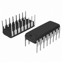
Package / Case
16-DIP (0.300", 7.62mm)
Current, Supply
120 μA
Function Type
6-Channels
Logic Function
Buffer
Number Of Circuits
Hex
Package Type
PDIP-16
Special Features
Non-Inverting, Tri-State
Temperature, Operating, Range
-55 to +125 °C
Voltage, Supply
3 to 18 VDC
Logic Family
4000
Logical Function
Buffer/Line Driver
Number Of Elements
2
Number Of Channels
6
Number Of Inputs
6
Number Of Outputs
6
Operating Supply Voltage (typ)
3.3/5/9/12/15V
Output Type
3-State
Polarity
Non-Inverting
Propagation Delay Time
200ns
High Level Output Current
-8.2mA
Low Level Output Current
19.2mA
Operating Supply Voltage (max)
18V
Operating Supply Voltage (min)
3V
Quiescent Current
4uA
Technology
CMOS
Pin Count
16
Mounting
Through Hole
Operating Temp Range
-55C to 125C
Operating Temperature Classification
Military
Number Of Channels Per Chip
5
Supply Voltage (max)
18 V
Supply Voltage (min)
3 V
Maximum Operating Temperature
+ 125 C
Mounting Style
Through Hole
Maximum Power Dissipation
500 mW
Minimum Operating Temperature
- 55 C
Number Of Lines (input / Output)
6 / 3
Logic Device Type
Buffer, Non Inverting
Supply Voltage Range
3V To 18V
Logic Case Style
DIP
No. Of Pins
16
Operating Temperature Range
-55°C To +125°C
Filter Terminals
DIP
Rohs Compliant
Yes
Family Type
4000 CMOS
Lead Free Status / RoHS Status
Lead free / RoHS Compliant
Other names
MC14503BCPGOS


†For information on tape and reel specifications, including part orientation and tape sizes, please refer to our Tape and Reel Packaging
ORDERING INFORMATION
Specifications Brochure, BRD8011/D.
MC14503BCP
MC14503BCPG
MC14503BD
MC14503BDG
MC14503BDR2
MC14503BDR2G
MC14503BFEL
MC14503BFELG
DISABLE B
DISABLE A
IN 5
IN 6
IN 1
IN 2
IN 3
IN 4
OUT 1
OUT 2
OUT 3
DIS A
IN 1
IN 2
IN 3
V
SS
15
12
14
10
LOGIC DIAGRAM
PIN ASSIGNMENT
2
4
6
1
1
2
3
4
5
6
7
8
V
Device
V
DD
SS
= PIN 16
= PIN 8
16
15
14
13
12
10
11
9
V
DIS B
IN 6
OUT 6
IN 5
OUT 5
IN 4
OUT 4
DD
11
13
3
5
7
9
OUT 5
OUT 6
OUT 1
OUT 2
OUT 3
OUT 4
http://onsemi.com
*DISABLE
*
*Diode protection on all inputs (not shown)
INPUT
MC14503B
*IN
n
TO OTHER BUFFERS
2
SOEIAJ−16
SOEIAJ−16
(Pb−Free)
(Pb−Free)
(Pb−Free)
(Pb−Free)
Package
SOIC−16
SOIC−16
SOIC−16
SOIC−16
PDIP−16
PDIP−16
X = Don’t Care
In
0
1
X
n
CIRCUIT DIAGRAM
Appropriate
TRUTH TABLE
Disable
Input
0
0
1
ONE OF TWO/FOUR BUFFERS
Impedance
Out
High
2500 / Tape & Reel
2000 / Tape & Reel
0
1
n
Shipping
25 / Rail
48 / Rail
†
V
V
SS
DD
OUT
n
Related parts for MC14503BCPG
Image
Part Number
Description
Manufacturer
Datasheet
Request
R

Part Number:
Description:
CONTACTOR, 1NO, 110VAC, 14A, DIN RAIL
Manufacturer:
IMO PRECISION CONTROLS
Datasheet:
Part Number:
Description:
CONTACTOR, 1NO, 230VAC, 14A, DIN RAIL
Manufacturer:
IMO PRECISION CONTROLS
Datasheet:
Part Number:
Description:
CONTACTOR, 1NO, 24VAC, 14A, DIN RAIL
Manufacturer:
IMO PRECISION CONTROLS
Datasheet:

Part Number:
Description:
ON Semiconductor [VOLTAGE REGULATOR]
Manufacturer:
ON Semiconductor
Datasheet:
Part Number:
Description:
357-036-542-201 CARDEDGE 36POS DL .156 BLK LOPRO
Manufacturer:
ON Semiconductor
Datasheet:
Part Number:
Description:
357-036-542-201 CARDEDGE 36POS DL .156 BLK LOPRO
Manufacturer:
ON Semiconductor
Datasheet:
Part Number:
Description:
357-036-542-201 CARDEDGE 36POS DL .156 BLK LOPRO
Manufacturer:
ON Semiconductor
Datasheet:
Part Number:
Description:
357-036-542-201 CARDEDGE 36POS DL .156 BLK LOPRO
Manufacturer:
ON Semiconductor
Datasheet:
Part Number:
Description:
357-036-542-201 CARDEDGE 36POS DL .156 BLK LOPRO
Manufacturer:
ON Semiconductor
Datasheet:
Part Number:
Description:
357-036-542-201 CARDEDGE 36POS DL .156 BLK LOPRO
Manufacturer:
ON Semiconductor
Datasheet:
Part Number:
Description:
357-036-542-201 CARDEDGE 36POS DL .156 BLK LOPRO
Manufacturer:
ON Semiconductor
Datasheet:
Part Number:
Description:
357-036-542-201 CARDEDGE 36POS DL .156 BLK LOPRO
Manufacturer:
ON Semiconductor
Datasheet:
Part Number:
Description:
357-036-542-201 CARDEDGE 36POS DL .156 BLK LOPRO
Manufacturer:
ON Semiconductor
Datasheet:
Part Number:
Description:
357-036-542-201 CARDEDGE 36POS DL .156 BLK LOPRO
Manufacturer:
ON Semiconductor
Datasheet: