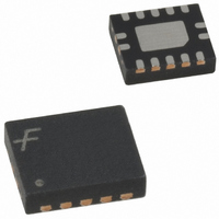
74LCX07BQX Fairchild Semiconductor, 74LCX07BQX Datasheet - Page 3

74LCX07BQX
Manufacturer Part Number
74LCX07BQX
Description
IC BUFF HEX LV OP/DRAIN 14DQFN
Manufacturer
Fairchild Semiconductor
Series
74LCXr
Datasheet
1.74LCX07MTCX.pdf
(12 pages)
Specifications of 74LCX07BQX
Logic Type
Buffer/Line Driver, Non-Inverting with Open Drain
Number Of Elements
6
Number Of Bits Per Element
1
Current - Output High, Low
32mA, 32mA
Voltage - Supply
2 V ~ 5.5 V
Operating Temperature
-40°C ~ 85°C
Mounting Type
Surface Mount
Package / Case
14-WQFN Exposed Pad, 14-DQFN
Logic Family
LCX
Number Of Channels Per Chip
5
Polarity
Non-Inverting
Supply Voltage (max)
5.5 V
Supply Voltage (min)
2 V
Maximum Operating Temperature
+ 85 C
Mounting Style
SMD/SMT
Low Level Output Current
32 mA
Minimum Operating Temperature
- 40 C
Number Of Lines (input / Output)
6 / 3
Output Type
Open Drain
Propagation Delay Time
4.4 ns at 2.7 V, 3.7 ns at 3.3 V, 3 ns at 5 V
Lead Free Status / RoHS Status
Lead free / RoHS Compliant
Available stocks
Company
Part Number
Manufacturer
Quantity
Price
Part Number:
74LCX07BQX
Manufacturer:
ON/ه®‰و£®ç¾ژ
Quantity:
20 000
©1999 Fairchild Semiconductor Corporation
74LCX07 Rev. 1.11.0
Absolute Maximum Ratings
Stresses exceeding the absolute maximum ratings may damage the device. The device may not function or be
operable above the recommended operating conditions and stressing the parts to these levels is not recommended.
In addition, extended exposure to stresses above the recommended operating conditions may affect device reliability.
The absolute maximum ratings are stress ratings only.
Note:
2. I
Recommended Operating Conditions
The Recommended Operating Conditions table defines the conditions for actual device operation. Recommended
operating conditions are specified to ensure optimal performance to the datasheet specifications. Fairchild does not
recommend exceeding them or designing to absolute maximum ratings.
Note:
3. Unused inputs must be held HIGH or LOW. They may not float.
Symbol
Symbol
O
T
I
V
V
t / V
I
GND
I
Absolute Maximum Rating must be observed.
V
V
I
I
STG
T
V
OK
I
CC
V
OL
CC
IK
CC
O
O
O
A
I
I
Supply Voltage
DC Input Voltage
DC Output Voltage, Output in HIGH or LOW State
DC Input Diode Current, V
DC Output Diode Current
DC Output Current
DC Supply Current per Supply Pin
DC Ground Current per Ground Pin
Storage Temperature
Supply Voltage
Input Voltage
Output Voltage
Output Current
Free-Air Operating Temperature
Input Edge Rate, V
V
V
Operating
Data Retention
V
V
V
V
O
O
CC
CC
CC
CC
V
GND
CC
4.5V–5.5V
3.0V–3.6V
2.7V–3.0V
2.3V–2.7V
IN
0.8V–2.0V, V
Parameter
I
GND
Parameter
CC
(3)
3.0V
3
(2)
Min.
–40
2.0
1.5
0
0
0
Max.
+32
+24
+12
5.5
5.5
5.5
5.5
+8
85
10
Rating
–65°C to +150°C
–0.5V to +7.0V
–0.5V to +7.0V
–0.5V to +7.0V
www.fairchildsemi.com
±100mA
±100mA
Units
ns / V
–50mA
–50mA
+50mA
±50mA
mA
°C
V
V
V


