74ACT899QC Fairchild Semiconductor, 74ACT899QC Datasheet

IC LATCH BIDIRECT 9-BIT 28-PLCC

74ACT899QC

Manufacturer Part Number
74ACT899QC
Description
IC LATCH BIDIRECT 9-BIT 28-PLCC
Manufacturer
Fairchild Semiconductor
Series
74ACTr
Datasheet

Specifications of 74ACT899QC

Logic Type
Transceiver, Non-Inverting
Number Of Elements
1
Number Of Bits Per Element
9
Current - Output High, Low
24mA, 24mA
Voltage - Supply
4.5 V ~ 5.5 V
Operating Temperature
-40°C ~ 85°C
Mounting Type
Surface Mount
Package / Case
28-PLCC
Lead Free Status / RoHS Status
Contains lead / RoHS non-compliant

Available stocks

Company
Part Number
Manufacturer
Quantity
Price
Part Number:
74ACT899QC
Manufacturer:
Fairchild Semiconductor
Quantity:
10 000
Part Number:
74ACT899QCX
Manufacturer:
FAIRCHILD/仙童
Quantity:
20 000
© 1999 Fairchild Semiconductor Corporation
74ACT899
9-Bit Latchable Transceiver with Parity
Generator/Checker
General Description
The ACT899 is a 9-bit to 9-bit parity transceiver with trans-
parent latches. The device can operate as a feed-through
transceiver or it can generate/check parity from the 8-bit
data busses in either direction. The ACT899 features inde-
pendent latch enables for the A-to-B direction and the B-to-
A direction, a select pin for ODD/EVEN parity, and sepa-
rate error signal output pins for checking parity.
Ordering Code:
Device also available in Tape and Reel. Specify by appending suffix letter “X” to the ordering code.
Logic Symbol
FACT
Order Number
74ACT899QC
is a trademark of Fairchild Semiconductor Corporation.
Package Number
V28A
28-Lead Plastic Lead Chip Carrier (PLCC), JEDEC MO-047, 0.450” Square
DS010637.prf
Features
Connection Diagram
Latchable transceiver with output sink of 24 mA
Option to select generate parity and check or
“feed-through” data/parity in directions A-to-B or B-to-A
Independent latch enable for A-to-B and B-to-A
directions
Select pin for ODD/EVEN parity
ERRA and ERRB output pins for parity checking
Ability to simultaneously generate and check parity
May be used in system applications in place of the 280
May be used in system applications in place of the 657
and 373 (no need to change T/R to check parity)
Package Description
Pin Assignment for PCC
January 1990
Revised December 1998
www.fairchildsemi.com

Related parts for 74ACT899QC

74ACT899QC Summary of contents

Page 1

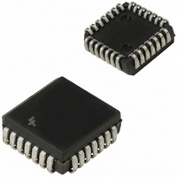
... Ordering Code: Order Number Package Number 74ACT899QC V28A 28-Lead Plastic Lead Chip Carrier (PLCC), JEDEC MO-047, 0.450” Square Device also available in Tape and Reel. Specify by appending suffix letter “X” to the ordering code. ...

Page 2

Pin Descriptions Pin Names Description A –A A Bus Data Inputs/Data Outputs –B B Bus Data Inputs/Data Outputs 0 7 APAR, BPAR A and B Bus Parity Inputs ODD/EVEN ODD/EVEN Parity Select, Active LOW for EVEN Parity ...

Page 3

Functional Block Diagram AC Path A , APAR B , BPAR BPAR A , APAR BPAR n (B APAR) n FIGURE 1. FIGURE 2. 3 www.fairchildsemi.com ...

Page 4

A ERRA n (B ERRB) n O/E ERRA O/E ERRB O/E BPAR (O/E APAR) www.fairchildsemi.com FIGURE 3. FIGURE 4. FIGURE 5. 4 ...

Page 5

APAR ERRA (BPAR ERRB) ZH, HZ ZL, LZ SEL BPAR (SEL APAR) FIGURE 6. FIGURE 7. FIGURE 8. FIGURE 9. 5 www.fairchildsemi.com ...

Page 6

LEA BPAR, B[0:7] (LEB APAR, A[0:7]) TS(H), TH(H) LEA APAR, A[0:7] (LEB BPAR, B[0:7]) TS(L), TH(L) LEA APAR, A[0:7] (LEB BPAR, B[0:7]) www.fairchildsemi.com FIGURE 10. FIGURE 11. FIGURE 12. FIGURE 13. 6 ...

Page 7

Absolute Maximum Ratings Supply Voltage ( Input Diode Current ( 0. 0. Input Voltage ( Output Diode Current ( ...

Page 8

AC Electrical Characteristics Symbol Parameter (Note 5) t Propagation Delay PLH PHL Propagation Delay PLH t APAR, BPAR to BPAR, APAR PHL t Propagation Delay PLH t ...

Page 9

Physical Dimensions inches (millimeters) unless otherwise noted 28-Lead Plastic Lead Chip Carrier (PLCC), JEDEC MO-047, 0.450” Square LIFE SUPPORT POLICY FAIRCHILD’S PRODUCTS ARE NOT AUTHORIZED FOR USE AS CRITICAL COMPONENTS IN LIFE SUPPORT DEVICES OR SYSTEMS WITHOUT THE EXPRESS WRITTEN ...

Related keywords