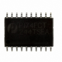
PI74FCT244ATSE Pericom Semiconductor, PI74FCT244ATSE Datasheet - Page 3

PI74FCT244ATSE
Manufacturer Part Number
PI74FCT244ATSE
Description
IC BUFF/DVR DUAL N-INV 20SOIC
Manufacturer
Pericom Semiconductor
Series
74FCTr
Datasheet
1.PI74FCT244ATQE.pdf
(8 pages)
Specifications of PI74FCT244ATSE
Logic Type
Buffer/Line Driver, Non-Inverting
Number Of Elements
2
Number Of Bits Per Element
4
Current - Output High, Low
15mA, 64mA
Voltage - Supply
4.75 V ~ 5.25 V
Operating Temperature
-40°C ~ 85°C
Mounting Type
Surface Mount
Package / Case
20-SOIC
Logic Family
FCT
Number Of Channels Per Chip
8
Polarity
Non-Inverting
Supply Voltage (max)
5.25 V
Supply Voltage (min)
4.75 V
Maximum Operating Temperature
+ 85 C
Mounting Style
SMD/SMT
High Level Output Current
- 15 mA
Low Level Output Current
64 mA
Minimum Operating Temperature
- 40 C
Number Of Lines (input / Output)
8 / 8
Output Type
3-State
Propagation Delay Time
4.8 ns at 5 V
Lead Free Status / RoHS Status
Lead free / RoHS Compliant
Maximum Ratings
(Above which the useful life may be impaired. For user guidelines, not tested.)
DC Electrical Characteristics (Over the Operating Range, TA = –40°C to +85°C, VCC = 5.0V ± 5%)
Notes:
1. For Max. or Min. conditions, use appropriate value specifi ed under Electrical Characteristics for the applicable device type.
2. Typical values are at Vcc = 5.0V, +25°C ambient and maximum loading.
3. Not more than one output should be shorted at one time. Duration of the test should not exceed one second.
Capacitance
Notes:
1. This parameter is determined by device characterization but is not production tested.
V
V
V
V
V
I
I
I
I
V
I
I
V
C
C
Storage Temperature ............................................................. –65°C to +150°C
Ambient Temperature with Power Applied .............................-40°C to +85°C
Supply Voltage to Ground Potential (Inputs & Vcc Only) ...... –0.5V to +7.0V
Supply Voltage to Ground Potential (Outputs & D/O Only) ... –0.5V to +7.0V
DC Input Voltage ..................................................................... –0.5V to +7.0V
DC Output Current ................................................................................ 120mA
Power Dissipation .................................................................................... 0.5W
Parameters
IH
IL
OZH
OZL
OFF
OS
IN
OUT
OH
OL
OL
IH
IL
IK
H
Parameters
08-0291
Output HIGH Voltage
Output LOW Current
Output LOW Current
Input HIGH Voltage
Input LOW Voltage
Input HIGH Current
Input LOW Current
High Impedance
Output Current
Clamp Diode Voltage
Power Down Disable
Short Circuit Current
Input Hysteresis
(T
A
(1)
= 25°C, f = 1 MHz)
De scrip tion
Input Capacitance
Output Capacitance
De scrip tion
V
V
V
Guaranteed Logic HIGH Level
Guaranteed Logic LOW Level
V
V
V
V
V
V
CC
CC
CC
CC
CC
CC
CC
CC
CC
= Min., V
= Min., V
= Min., V
= Max.
= Max.
= M
= Min., I
= GND, V
= Max.
AX
.
(3)
IN
, V
IN
IN
IN
OUT
= –18mA
Test Conditions
= V
= V
= V
OUT
= 4.5V
V
V
IH
IH
IH
= GND
IN
OUT
or V
or V
or V
= 0V
3
= 0V
IL
IL
IL
Test Conditions
(1)
I
I
I
(25ΩSeries)
V
V
V
V
OH
OL
OL
IN
IN
OUT
OUT
Note:
Stresses greater than those listed under MAX I MUM
RATINGS may cause permanent damage to the
device. This is a stress rating only and functional
op er a tion of the device at these or any other con-
di tions above those indicated in the operational
sections of this specifi cation is not implied. Exposure to
absolute maximum rating conditions for extended periods
may affect re li abil i ty.
= 64mA
= 12mA
= –15.0mA
Fast CMOS Non-Inverting Octal Buffer/Line Drivers
= V
= GND
= 2.7V
= 0.5V
CC
Min.
–60
2.4
2.0
Typ.
8
6
Typ
–120
–0.7
200
3.0
0.3
0.3
(2)
Max.
PI74FCT244T/2244T
PI74FCT541T/2541T
10
12
PS2011G
Max.
0.55
0.50
–1.2
100
0.8
–1
–1
1
1
Units
pF
Units
mA
μA
μA
11/10/08
V
V


