MC74VHCT50ADTR2G ON Semiconductor, MC74VHCT50ADTR2G Datasheet
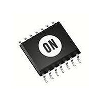
IC BUFF/LVL SHFTR N-INV 14TSSOP

MC74VHCT50ADTR2G

Manufacturer Part Number
MC74VHCT50ADTR2G
Description
IC BUFF/LVL SHFTR N-INV 14TSSOP
Manufacturer
ON Semiconductor
Series
74VHCTr
Datasheet

Specifications of MC74VHCT50ADTR2G

Logic Type
Buffer/Line Driver, Non-Inverting
Number Of Elements
6
Number Of Bits Per Element
1
Current - Output High, Low
8mA, 8mA
Voltage - Supply
2 V ~ 5.5 V
Operating Temperature
-55°C ~ 125°C
Mounting Type
Surface Mount
Package / Case
14-TSSOP
Logic Family
74VHC
Number Of Channels Per Chip
Hex
Polarity
Non-Inverting
Supply Voltage (max)
5.5 V
Supply Voltage (min)
2 V
Maximum Operating Temperature
125 C
Mounting Style
SMD/SMT
High Level Output Current
- 8 mA
Input Bias Current (max)
2 uA
Low Level Output Current
8 mA
Maximum Power Dissipation
450 mW
Minimum Operating Temperature
- 55 C
Number Of Lines (input / Output)
3
Propagation Delay Time
11.4 ns @ 3.3 V or 8.5 ns @ 5 V
Lead Free Status / RoHS Status
Lead free / RoHS Compliant
Other names
MC74VHCT50ADTR2GOS
MC74VHCT50ADTR2GOS
MC74VHCT50ADTR2GOSTR

Available stocks

Company
Part Number
Manufacturer
Quantity
Price
Part Number:
MC74VHCT50ADTR2G
Manufacturer:
ON
Quantity:
2 500
Part Number:
MC74VHCT50ADTR2G
Manufacturer:
MICREL
Quantity:
206
Part Number:
MC74VHCT50ADTR2G
Manufacturer:
ON/安森美
Quantity:
20 000
Part Number:
MC74VHCT50ADTR2G
0
MC74VHCT50A
Noninverting Buffer /
CMOS Logic Level Shifter
with LSTTL−Compatible Inputs
silicon gate CMOS technology. It achieves high speed operation
similar to equivalent Bipolar Schottky TTL while maintaining CMOS
low power dissipation.
output which provides high noise immunity and stable output.
the output has a full 5 V CMOS level output swing. The input
protection circuitry on this device allows overvoltage tolerance on the
input, allowing the device to be used as a logic−level translator from
3.0 V CMOS logic to 5.0 V CMOS Logic or from 1.8 V CMOS logic
to 3.0 V CMOS Logic while operating at the high−voltage power
supply.
voltages up to 7 V are applied, regardless of the supply voltage. This
allows the MC74VHCT50A to be used to interface 5 V circuits to 3 V
circuits. The output structures also provide protection when
V
destruction caused by supply voltage − input/output voltage mismatch,
battery backup, hot insertion, etc.
© Semiconductor Components Industries, LLC, 2007
January, 2007− Rev. 6
CC
A1
A2
A3
A4
A5
A6
The MC74VHCT50A is a hex noninverting buffer fabricated with
The internal circuit is composed of three stages, including a buffered
The device input is compatible with TTL−type input thresholds and
The MC74VHCT50A input structure provides protection when
High Speed: t
Low Power Dissipation: I
TTL−Compatible Inputs: V
CMOS−Compatible Outputs: V
Power Down Protection Provided on Inputs and Outputs
Pb−Free Packages are Available
= 0 V. These input and output structures help prevent device
1
3
5
9
11
13
LOGIC DIAGRAM
PD
= 3.5 ns (Typ) at V
10
12
2
4
6
8
Y1
Y2
Y3
Y4
Y5
Y6
CC
Y = A
IL
= 2 mA (Max) at T
= 0.8 V; V
OH
> 0.8 V
CC
A1
A2
A3
A4
A5
A6
= 5 V
IH
LOGIC SYMBOL
CC
= 2.0 V
; V
A
OL
= 25°C
< 0.1 V
1
1
1
1
1
1
1
CC
@Load
Y1
Y2
Y3
Y4
Y5
Y6
For detailed package marking information, see the Marking
Diagram section on page 4 of this data sheet.
See detailed ordering and shipping information in the package
dimensions section on page 4 of this data sheet.
14−LEAD SOIC
V
14
A1
1
CASE 751A
CC
MARKING DIAGRAM (Top View)
D SUFFIX
A Input
ORDERING INFORMATION
PIN CONNECTION AND
H
L
A6
Y1
13
2
http://onsemi.com
FUNCTION TABLE
14−LEAD SOIC EIAJ
Y6
A2
12
3
M SUFFIX
CASE 965
A5
Y2
11
Publication Order Number:
4
14−LEAD TSSOP
Y5
A3
10
5
CASE 948G
MC74VHCT50A/D
DT SUFFIX
Y Output
A4
Y3
9
6
H
L
GND
Y4
8
7

Related parts for MC74VHCT50ADTR2G

MC74VHCT50ADTR2G Summary of contents

Page 1

MC74VHCT50A Noninverting Buffer / CMOS Logic Level Shifter with LSTTL−Compatible Inputs The MC74VHCT50A is a hex noninverting buffer fabricated with silicon gate CMOS technology. It achieves high speed operation similar to equivalent Bipolar Schottky TTL while maintaining CMOS low power ...

Page 2

MAXIMUM RATINGS Symbol V DC Supply Voltage Input Voltage Output Voltage OUT I DC Input Diode Current Output Diode Current Output Source/Sink Current Supply Current ...

Page 3

DC ELECTRICAL CHARACTERISTICS Symbol Parameter V Minimum High−Level IH Input Voltage V Maximum Low−Level IL Input Voltage V Minimum High−Level OH Output Voltage Maximum Low−Level OL Output Voltage ...

Page 4

... ORDERING INFORMATION Device MC74VHCT50AD MC74VHCT50ADG MC74VHCT50ADR2 MC74VHCT50ADR2G MC74VHCT50ADT MC74VHCT50ADTG MC74VHCT50ADTR2 MC74VHCT50ADTR2G MC74VHCT50AM MC74VHCT50AMG MC74VHCT50AMEL MC74VHCT50AMELG †For information on tape and reel specifications, including part orientation and tape sizes, please refer to our Tape and Reel Packaging Specifications Brochure, BRD8011/ VHCT50AG AWLYWW 14−LEAD SOIC ...

Page 5

G −T− K SEATING PLANE 0.25 (0.010 14X 0.58 MC74VHCT50A PACKAGE DIMENSIONS D SUFFIX PLASTIC SOIC PACKAGE CASE 751A−03 ISSUE 0.25 (0.010 ...

Page 6

K 14X REF 0.10 (0.004) 0.15 (0.006 L PIN 1 IDENT. 1 0.15 (0.006 −V− C 0.10 (0.004) SEATING −T− PLANE 14X 0.36 MC74VHCT50A PACKAGE DIMENSIONS DT SUFFIX ...

Page 7

... Opportunity/Affirmative Action Employer. This literature is subject to all applicable copyright laws and is not for resale in any manner. PUBLICATION ORDERING INFORMATION LITERATURE FULFILLMENT: Literature Distribution Center for ON Semiconductor P.O. Box 5163, Denver, Colorado 80217 USA Phone: 303−675−2175 or 800−344−3860 Toll Free USA/Canada Fax: 303− ...

Related keywords