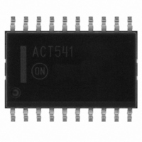
MC74ACT541DWR2G ON Semiconductor, MC74ACT541DWR2G Datasheet - Page 2

MC74ACT541DWR2G
Manufacturer Part Number
MC74ACT541DWR2G
Description
IC BUFF/DVR TRI-ST 8BIT 20SOIC
Manufacturer
ON Semiconductor
Series
74ACTr
Datasheet
1.MC74ACT541NG.pdf
(12 pages)
Specifications of MC74ACT541DWR2G
Logic Type
Buffer/Line Driver, Non-Inverting
Number Of Elements
1
Number Of Bits Per Element
8
Current - Output High, Low
24mA, 24mA
Voltage - Supply
4.5 V ~ 5.5 V
Operating Temperature
-40°C ~ 85°C
Mounting Type
Surface Mount
Package / Case
20-SOIC (7.5mm Width)
Logic Family
74ACT
Number Of Channels Per Chip
Octal
Polarity
Non-Inverting
Supply Voltage (max)
5.5 V
Supply Voltage (min)
4.5 V
Maximum Operating Temperature
85 C
Mounting Style
SMD/SMT
High Level Output Current
- 24 mA
Input Bias Current (max)
8 uA
Low Level Output Current
24 mA
Maximum Power Dissipation
500 mW
Minimum Operating Temperature
- 40 C
Number Of Lines (input / Output)
3
Output Type
3-State
Propagation Delay Time
7.5 ns @ 5 V
Logical Function
Buffer/Line Driver
Number Of Elements
1
Number Of Channels
8
Number Of Inputs
8
Number Of Outputs
8
Operating Supply Voltage (typ)
5V
Package Type
SOIC W
Operating Supply Voltage (max)
5.5V
Operating Supply Voltage (min)
4.5V
Quiescent Current
8uA
Technology
CMOS
Pin Count
20
Mounting
Surface Mount
Operating Temp Range
-40C to 85C
Operating Temperature Classification
Industrial
Lead Free Status / RoHS Status
Lead free / RoHS Compliant
Other names
MC74ACT541DWR2GOS
MC74ACT541DWR2GOS
MC74ACT541DWR2GOSTR
MC74ACT541DWR2GOS
MC74ACT541DWR2GOSTR
Available stocks
Company
Part Number
Manufacturer
Quantity
Price
Company:
Part Number:
MC74ACT541DWR2G
Manufacturer:
ON Semiconductor
Quantity:
2 450
Stresses exceeding Maximum Ratings may damage the device. Maximum Ratings are stress ratings only. Functional operation above the
Recommended Operating Conditions is not implied. Extended exposure to stresses above the Recommended Operating Conditions may affect
device reliability.
1. V
2. V
MAXIMUM RATINGS
RECOMMENDED OPERATING CONDITIONS
V
Symbol
Symbol
IN
V
I
V
V
T
V
OUT
I
, V
t
t
I
IN
IN
I
OUT
I
r
r
T
T
CC
OH
OL
IN
stg
, t
, t
CC
CC
IN
A
J
from 30% to 70% V
from 0.8 V to 2.0 V; see individual Data Sheets for devices that differ from the typical input rise and fall times.
OUT
f
f
DC Supply Voltage (Referenced to GND)
DC Input Voltage (Referenced to GND)
DC Output Voltage (Referenced to GND)
DC Input Current, per Pin
DC Output Sink/Source Current, per Pin
DC V
Storage Temperature
Supply Voltage
DC Input Voltage, Output Voltage (Ref. to GND)
Input Rise and Fall Time (Note 1)
′AC Devices except Schmitt Inputs
Input Rise and Fall Time (Note 2)
′ACT Devices except Schmitt Inputs
Junction Temperature (PDIP)
Operating Ambient Temperature Range
Output Current − High
Output Current − Low
CC
Figure 1. MC74AC540/74ACT540
GND
OE
or GND Current per Output Pin
1
MC74AC540, MC74ACT540, MC74AC541, MC74ACT541
CC
10
1
2
3
4
5
6
7
8
9
; see individual Data Sheets for devices that differ from the typical input rise and fall times.
Parameter
Parameter
20
19
18
17
16
15
14
13
12
11
V
OE
CC
http://onsemi.com
2
2
Figure 2. MC74AC541/74ACT541
GND
OE
V
V
V
V
V
CC
CC
CC
CC
CC
1
′ACT
′AC
@ 3.0 V
@ 4.5 V
@ 5.5 V
@ 4.5 V
@ 5.5 V
10
1
2
3
4
5
6
7
8
9
Min
−40
2.0
4.5
0
−
−
−
−
−
−
−
−
−0.5 to V
−0.5 to V
−0.5 to +7.0
−65 to +150
20
19
18
17
16
15
14
13
12
11
Value
Typ
150
±20
±50
±50
5.0
5.0
8.0
40
25
10
25
−
−
−
−
CC
CC
V
OE
CC
+0.5
+0.5
2
Max
V
140
−24
6.0
5.5
85
24
−
−
−
−
−
CC
Unit
Unit
ns/V
ns/V
mA
mA
mA
mA
mA
°C
°C
°C
V
V
V
V
V


