MC14017B
Decade Counter
built−in code converter. High speed operation and spike−free outputs
are obtained by use of a Johnson decade counter design. The ten
decoded outputs are normally low, and go high only at their
appropriate decimal time period. The output changes occur on the
positive−going edge of the clock pulse. This part can be used in
frequency division applications as well as decade counter or decimal
decode display applications.
Features
•
•
•
•
•
•
•
•
•
Maximum ratings are those values beyond which device damage can occur.
Maximum ratings applied to the device are individual stress limit values (not
normal operating conditions) and are not valid simultaneously. If these limits are
exceeded, device functional operation is not implied, damage may occur and
reliability may be affected.
1. Temperature Derating:
static voltages or electric fields. However, precautions must be taken to avoid
applications of any voltage higher than maximum rated voltages to this
high−impedance circuit. For proper operation, V
to the range V
(e.g., either V
*For additional information on our Pb−Free strategy and soldering details, please
MAXIMUM RATINGS
© Semiconductor Components Industries, LLC, 2005
Symbol
V
download the ON Semiconductor Soldering and Mounting Techniques
Reference Manual, SOLDERRM/D.
I
The MC14017B is a five−stage Johnson decade counter with
in
This device contains protection circuitry to guard against damage due to high
Unused inputs must always be tied to an appropriate logic voltage level
Schottky TTL Load Over the Rated Temperature Range
in
Fully Static Operation
DC Clock Input Circuit Allows Slow Rise Times
Carry Out Output for Cascading
Divide−by−N Counting
Supply Voltage Range = 3.0 Vdc to 18 Vdc
Capable of Driving Two Low−Power TTL Loads or One Low−Power
Pin−for−Pin Replacement for CD4017B
Triple Diode Protection on All Inputs
Pb−Free Packages are Available*
V
T
Plastic “P and D/DW” Packages: – 7.0 mW/_C From 65_C To 125_C
P
, V
, I
T
T
stg
DD
A
D
L
out
out
DC Supply Voltage Range
Input or Output Voltage Range
Input or Output Current
Power Dissipation, per Package
Ambient Temperature Range
Storage Temperature Range
Lead Temperature
SS
SS
(DC or Transient)
(DC or Transient) per Pin
(Note 1)
(8−Second Soldering)
or V
v (V
DD
in
). Unused outputs must be left open.
Parameter
or V
(Voltages Referenced to V
out
) v V
DD
.
in
and V
−0.5 to V
SS
−0.5 to +18.0
−55 to +125
−65 to +150
out
)
Value
± 10
500
260
should be constrained
DD
+ 0.5
1
Unit
mW
mA
°C
°C
°C
V
V
See detailed ordering and shipping information in the package
dimensions section on page 3 of this data sheet.
ORDERING INFORMATION
A
WL, L
YY, Y
WW, W
G
CASE 751B
SOEIAJ−16
CASE 648
CASE 966
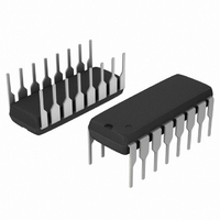
P SUFFIX
D SUFFIX
F SUFFIX
PDIP−16
SOIC−16
= Assembly Location
= Wafer Lot
= Year
= Work Week
= Pb−Free Indicator
Publication Order Number:
16
1
16
16
1
1
DIAGRAMS
MARKING
MC14017BCP
AWLYYWWG
MC14017B
AWLYWW
MC14017B/D
14017BG
ALYWG