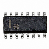
MC74HC4060ADR2 ON Semiconductor, MC74HC4060ADR2 Datasheet - Page 9

MC74HC4060ADR2
Manufacturer Part Number
MC74HC4060ADR2
Description
IC COUNTER OSC 14STAGE 16SOIC
Manufacturer
ON Semiconductor
Series
74HCr
Datasheet
1.MC74HC4060ADR2.pdf
(14 pages)
Specifications of MC74HC4060ADR2
Logic Type
Binary Counter
Direction
Up
Number Of Elements
1
Number Of Bits Per Element
14
Reset
Asynchronous
Count Rate
50MHz
Trigger Type
Negative Edge
Voltage - Supply
2 V ~ 6 V
Operating Temperature
-55°C ~ 125°C
Mounting Type
Surface Mount
Package / Case
16-SOIC (3.9mm Width)
Lead Free Status / RoHS Status
Contains lead / RoHS non-compliant
Timing
-
Other names
MC74HC4060ADROSCT
Available stocks
Company
Part Number
Manufacturer
Quantity
Price
Part Number:
MC74HC4060ADR2G
Manufacturer:
ON/安森美
Quantity:
20 000
impedance elements should be considered: C
180 C.
Reactance jX
The maximum R
the gain of the HC4060A amplifier.
capacitance of 32pF at the required frequency.
100,000. In-circuit Q is arbitrarily set at 20% below crystal Q or 80,000. Then R
crystal parameters.
Here R = R
Q = 2 f
CHOOSING R1
crystal. The drive level specified by the crystal manufacturer
is the maximum stress that a crystal can withstand without
damage or excessive shift in frequency. R1 limits the drive
level.
overdrive the crystal, monitor the output frequency as a
function of voltage at Osc Out 2 (Pin 9). The frequency
should increase very slightly as the dc supply voltage is
increased. An overdriven crystal will decrease in frequency
or become unstable with an increase in supply voltage. The
operating supply voltage must be reduced or R1 must be
increased in value if the overdriven condition exists. The
user should note that the oscillator start-up time is
proportional to the value of R1.
determines the gain and bandwidth of the amplifier. Proper
bandwidth insures oscillation at the correct frequency plus
roll-off to minimize gain at undesirable frequencies, such as
SELECTING R
The following procedure applies for oscillators operating below 2MHz where Z is a resistor R1. Above 2MHz, additional
Step 1: Calculate the equivalent series circuit of the crystal at the frequency of oscillation.
Step 2: Determine , the attenuation, of the feedback network. For a closed-loop gain of 2,A
Step 3: Determine the manufacturer’s loading capacitance. For example: A manufacturer may specify an external load
Step 4: Determine the required Q of the system, and calculate R
Step 5: Simultaneously solve, using a computer,
Alternately, pick a value for R1 (i.e, let R1 = R
Power is dissipated in the effective series resistance of the
To verify that the maximum dc supply voltage does not
The feedback resistor, R
Z e +
b +
X e + X C2 ) X C )
R load +
R @ R e ) X C2 (X e * X C )
o
L
* jX C o ) R s ) jX L s * jX C s
* jX C o (R s ) jX L s * jX C s )
s
/(R
out
RX C o X C2 [(X C ) X C2 )(X C ) X C o ) * X C (X C ) X C o ) X C2 )]
e
s
should be positive, indicating that the crystal is operating as an inductive reactance at the oscillation frequency.
+ R1. R
X C @ X C2
+ R
f
s
for the crystal should be used in the equation.
load
X 2 C2 (X C ) X C o ) 2 ) R 2 (X C ) X C o ) X C2 ) 2
out
) to find in-circuit Q. If Q is not satisfactory pick another value for R1 and repeat the procedure.
R e X C2
is amp output resistance, R1 is Z. The C corresponding to X
f
R
, typically ranges up to 20MW. R
+ X C load
(with feedback phase shift = 180 )
+ R e ) jX e
(where the loading capacitor is an external load, not including C
out
DESIGN PROCEDURES
and C
S
). Solve Equations 1 and 2 for C1 and C2. Use Equation 3 and the fact that
http://onsemi.com
MC74HC4060A
a
of the amp, feedback resistor R
f
9
the first overtone. R
the phase of the feedback network in an appreciable manner.
data sheet and are hereby acknowledged and recommended
for reading:
Design, March 7, 1985.
Machine Design, April 25, 1985.
ALSO RECOMMENDED FOR READING:
and Method of Measurement”, Proc. IEEE, Vol. 57, No. 2,
Feb., 1969.
Control”, Electro-Technology, June, 1969.
Design, May, 1966.
load
The following publications were used in preparing this
Technical Note TN-24, Statek Corp.
Technical Note TN-7, Statek Corp.
D. Babin, “Designing Crystal Oscillators”, Machine
E. Hafner, “The Piezoelectric Crystal Unit-Definitions
D. Kemper, L. Rosine, “Quartz Crystals for Frequency
P. J. Ottowitz, “A Guide to Crystal Selection”, Electronic
D. Babin, “Guidelines for Crystal Oscillator Design”,
ACKNOWLEDGEMENTS AND RECOMMENDED
, For example, a manufacturer specifies a crystal Q of
load
f
= (2 f
must be large enough so as to not affect
C
f
REFERENCES
, and amplifier phase shift error from
is given by C = C1 + C
o
L
S
/Q) − R
= 2, = 2/A where A is
s
where L
o
)
in
s
.
and R
( Eq 1 )
( Eq 2 )
( Eq 3 )
s
are


