MC74HC4060ANG ON Semiconductor, MC74HC4060ANG Datasheet - Page 4
MC74HC4060ANG
Manufacturer Part Number
MC74HC4060ANG
Description
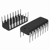
IC COUNTER 14STAGE BIN 16-DIP
Manufacturer
ON Semiconductor
Series
74HCr
Type
Binaryr
Specifications of MC74HC4060ANG
Logic Type
Binary Counter
Direction
Up
Number Of Elements
1
Number Of Bits Per Element
14
Reset
Asynchronous
Count Rate
50MHz
Trigger Type
Negative Edge
Voltage - Supply
2 V ~ 6 V
Operating Temperature
-55°C ~ 125°C
Mounting Type
Through Hole
Package / Case
16-DIP (0.300", 7.62mm)
Circuit Type
Silicon Gate
Current, Supply
160 μA
Function Type
14-Stages
Logic Function
Counter
Package Type
PDIP-16
Special Features
Binary, Ripple
Temperature, Operating, Range
-55 to +125 °C
Voltage, Supply
2 to 6 V
Technology
CMOS
Number Of Elements
1
Number Of Bits
14
Logic Family
HC
Logical Function
Counter
Operating Supply Voltage (typ)
2.5/3.3/5V
Propagation Delay Time
1000ns
Operating Temp Range
-55C to 125C
Operating Supply Voltage (min)
2V
Operating Supply Voltage (max)
6V
Operating Temperature Classification
Military
Mounting
Through Hole
Pin Count
16
Lead Free Status / RoHS Status
Lead free / RoHS Compliant
Timing
-
Lead Free Status / Rohs Status
RoHS Compliant part
Electrostatic Device
Other names
MC74HC4060ANGOS
Available stocks
Company
Part Number
Manufacturer
Quantity
Price
Company:

Part Number:
MC74HC4060ANG
Manufacturer:
ON Semiconductor
Quantity:
2 400


NOTE: Information on typical parametric values can be found in Chapter 2 of the ON Semiconductor High−Speed CMOS Data Book
DC CHARACTERISTICS
AC CHARACTERISTICS
Symbol
Symbol
Symbol
t
t
t
V
t
t
t
t
V
V
f
PLH
PLH
PLH
I
max
PHL
PHL
PHL
PHL
I
CC
OH
OL
OL
in
,
,
,
(DL129/D).
Maximum Low−Level Output Voltage
(Q4−Q10, Q12−Q14)
Minimum High−Level Output Voltage
(Osc Out 1, Osc Out 2)
Maximum Low−Level Output Voltage
(Osc Out 1, Osc Out 2)
Maximum Input Leakage Current
Maximum Quiescent Supply
Current (per Package)
Maximum Clock Frequency (50% Duty Cycle)
(Figures 1 and 4)
Maximum Propagation Delay, Osc In to Q4*
(Figures 1 and 4)
Maximum Propagation Delay, Osc In to Q14*
(Figures 1 and 4)
Maximum Propagation Delay, Reset to Any Q
(Figures 2 and 4)
Maximum Propagation Delay, Qn to Qn+1
(Figures 3 and 4)
Parameter
Parameter
(Voltages Referenced to GND)
(C
L
= 50 pF, Input t
Parameter
r
= t
V
|I
V
V
|I
V
V
|I
V
V
V
I
out
out
out
out
in
in
in
in
in
in
in
in
f
= 6 ns)
= V
= V
= V
=V
= V
=V
= V
= V
|
|
|
= 0mA
CC
CC
20mA
20mA
20mA
IH
IH
CC
CC
CC
CC
http://onsemi.com
MC74HC4060A
or V
or V
or GND
or GND
or GND
or GND
or GND
or GND
Condition
Condition
IL
IL
4
|I
|I
|I
|I
|I
|I
|I
|I
|I
out
out
out
out
out
out
out
out
out
|
|
|
|
|
|
|
|
|
2.4mA
4.0mA
5.2mA
0.7mA
1.0mA
1.3mA
0.7mA
1.0mA
1.3mA
V
V
V
2.0
4.5
6.0
3.0
4.5
6.0
2.0
4.5
6.0
3.0
4.5
6.0
2.0
4.5
6.0
3.0
4.5
6.0
6.0
6.0
2.0
3.0
4.5
6.0
2.0
3.0
4.5
6.0
2.0
3.0
4.5
6.0
2.0
3.0
4.5
6.0
2.0
3.0
4.5
6.0
V
V
V
CC
CC
CC
−55 to 25 C
−55 to 25 C
0.26
0.26
0.26
2.48
3.98
5.48
0.26
0.26
0.26
300
180
500
350
250
200
195
0.1
0.1
0.1
1.9
4.4
5.9
0.1
0.1
0.1
6.0
10
30
50
60
51
75
39
33
75
60
15
13
0.1
4
Guaranteed Limit
Guaranteed Limit
0.33
0.33
0.33
2.34
3.84
5.34
0.33
0.33
0.33
85 C
85 C
375
200
750
450
275
220
245
100
0.1
0.1
0.1
1.9
4.4
5.9
0.1
0.1
0.1
9.0
40
14
28
45
75
64
49
42
95
75
19
16
1.0
125 C
125 C
1000
0.40
0.40
0.40
2.20
3.70
5.20
0.40
0.40
0.40
160
450
250
600
300
250
300
125
125
0.1
0.1
0.1
1.9
4.4
5.9
0.1
0.1
0.1
8.0
12
25
40
90
75
61
53
95
24
20
1.0
MHz
Unit
Unit
Unit
mA
mA
ns
ns
ns
ns
V
V
V
Related parts for MC74HC4060ANG
Image
Part Number
Description
Manufacturer
Datasheet
Request
R

Part Number:
Description:
ON Semiconductor [VOLTAGE REGULATOR]
Manufacturer:
ON Semiconductor
Datasheet:
Part Number:
Description:
357-036-542-201 CARDEDGE 36POS DL .156 BLK LOPRO
Manufacturer:
ON Semiconductor
Datasheet:
Part Number:
Description:
357-036-542-201 CARDEDGE 36POS DL .156 BLK LOPRO
Manufacturer:
ON Semiconductor
Datasheet:
Part Number:
Description:
357-036-542-201 CARDEDGE 36POS DL .156 BLK LOPRO
Manufacturer:
ON Semiconductor
Datasheet:
Part Number:
Description:
357-036-542-201 CARDEDGE 36POS DL .156 BLK LOPRO
Manufacturer:
ON Semiconductor
Datasheet:
Part Number:
Description:
357-036-542-201 CARDEDGE 36POS DL .156 BLK LOPRO
Manufacturer:
ON Semiconductor
Datasheet:
Part Number:
Description:
357-036-542-201 CARDEDGE 36POS DL .156 BLK LOPRO
Manufacturer:
ON Semiconductor
Datasheet:
Part Number:
Description:
357-036-542-201 CARDEDGE 36POS DL .156 BLK LOPRO
Manufacturer:
ON Semiconductor
Datasheet:
Part Number:
Description:
357-036-542-201 CARDEDGE 36POS DL .156 BLK LOPRO
Manufacturer:
ON Semiconductor
Datasheet:
Part Number:
Description:
357-036-542-201 CARDEDGE 36POS DL .156 BLK LOPRO
Manufacturer:
ON Semiconductor
Datasheet:
Part Number:
Description:
357-036-542-201 CARDEDGE 36POS DL .156 BLK LOPRO
Manufacturer:
ON Semiconductor
Datasheet:
Part Number:
Description:
Manufacturer:
ON Semiconductor
Datasheet:
Part Number:
Description:
Manufacturer:
ON Semiconductor
Datasheet:
Part Number:
Description:
Manufacturer:
ON Semiconductor
Datasheet: