DM74LS191N Fairchild Semiconductor, DM74LS191N Datasheet

IC COUNTER BINARY UP/DOWN 16-DIP

DM74LS191N

Manufacturer Part Number
DM74LS191N
Description
IC COUNTER BINARY UP/DOWN 16-DIP
Manufacturer
Fairchild Semiconductor
Series
74LSr
Datasheet

Specifications of DM74LS191N

Logic Type
Binary Counter
Direction
Up, Down
Number Of Elements
1
Number Of Bits Per Element
4
Timing
Synchronous
Count Rate
20MHz
Trigger Type
Positive Edge
Voltage - Supply
4.75 V ~ 5.25 V
Operating Temperature
0°C ~ 70°C
Mounting Type
Through Hole
Package / Case
16-DIP (0.300", 7.62mm)
Lead Free Status / RoHS Status
Contains lead / RoHS non-compliant
Reset
-
Other names
74LS191
74LS191N
© 1999 Fairchild Semiconductor Corporation
Order Number
DM74LS191M
DM74LS191N
DM74LS191
Synchronous 4-Bit Up/Down Counter with Mode Control
General Description
The DM74LS191 circuit is a synchronous, reversible, up/
down counter. Synchronous operation is provided by hav-
ing all flip-flops clocked simultaneously, so that the outputs
change simultaneously when so instructed by the steering
logic. This mode of operation eliminates the output count-
ing spikes normally associated with asynchronous (ripple
clock) counters.
The outputs of the four master-slave flip-flops are triggered
on a LOW-to-HIGH level transition of the clock input, if the
enable input is LOW. A HIGH at the enable input inhibits
counting. Level changes at either the enable input or the
down/up input should be made only when the clock input is
HIGH. The direction of the count is determined by the level
of the down/up input. When LOW, the counter counts up
and when HIGH, it counts down.
The counter is fully programmable; that is, the outputs may
be preset to either level by placing a LOW on the load input
and entering the desired data at the data inputs. The output
will change independent of the level of the clock input. This
feature allows the counters to be used as modulo-N divid-
ers by simply modifying the count length with the preset
inputs.
The clock, down/up, and load inputs are buffered to lower
the drive requirement; which significantly reduces the num-
ber of clock drivers, etc., required for long parallel words.
Ordering Code:
Devices also available in Tape and Reel. Specify by appending the suffix letter “X” to the ordering code.
Package Number
M16A
N16E
16-Lead Small Outline Integrated Circuit (SOIC), JEDEC MS-012, 0.150” Narrow Body
16-Lead Plastic Dual-In-Line Package (PDIP), JEDEC MS-001, 0.300” Wide
DS006405.prf
Two outputs have been made available to perform the cas-
cading function: ripple clock and maximum/minimum count.
The latter output produces a high-level output pulse with a
duration approximately equal to one complete cycle of the
clock when the counter overflows or underflows. The ripple
clock output produces a low-level output pulse equal in
width to the low-level portion of the clock input when an
overflow or underflow condition exists. The counters can be
easily cascaded by feeding the ripple clock output to the
enable input of the succeeding counter if parallel clocking
is used, or to the clock input if parallel enabling is used.
The maximum/minimum count output can be used to
accomplish look-ahead for high-speed operation.
Features
Counts binary
Single down/up count control line
Count enable control input
Ripple clock output for cascading
Asynchronously presettable with load control
Parallel outputs
Cascadable for n-bit applications
Average propagation delay 20 ns
Typical clock frequency 25 MHz
Typical power dissipation 100 mW
Package Description
August 1986
Revised February 1999
www.fairchildsemi.com

Related parts for DM74LS191N

DM74LS191N Summary of contents

Page 1

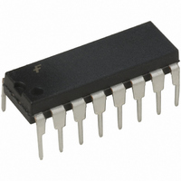
... DM74LS191M M16A 16-Lead Small Outline Integrated Circuit (SOIC), JEDEC MS-012, 0.150” Narrow Body DM74LS191N N16E 16-Lead Plastic Dual-In-Line Package (PDIP), JEDEC MS-001, 0.300” Wide Devices also available in Tape and Reel. Specify by appending the suffix letter “X” to the ordering code. ...

Page 2

Connection Diagram Timing Diagram www.fairchildsemi.com 2 ...

Page 3

Logic Diagram Pin (16 Pin (8) GND CC 3 www.fairchildsemi.com ...

Page 4

Absolute Maximum Ratings Storage Temperature Range Input Voltage Operating Free Air Temp. Range Supply Voltage Recommended Operating Conditions Symbol V Supply Voltage CC V HIGH Level Input Voltage IH V LOW Level Input Voltage IL I HIGH Level Output Current ...

Page 5

AC Electrical Characteristics Symbol Parameter f Maximum Clock MAX Frequency t Propagation Delay Time PLH LOW-to-HIGH Level Output t Propagation Delay Time PHL HIGH-to-LOW Level Output t Propagation Delay Time PLH LOW-to-HIGH Level Output t Propagation Delay Time PHL HIGH-to-LOW ...

Page 6

Physical Dimensions inches (millimeters) unless otherwise noted 16-Lead Small Outline Integrated Circuit (SOIC), JEDEC MS012, 0.150” Narrow Body 16-Lead Plastic Dual-In-Line Package (PDIP), JEDEC MS-001, 300” Wide LIFE SUPPORT POLICY FAIRCHILD’S PRODUCTS ARE NOT AUTHORIZED FOR USE AS CRITICAL COMPONENTS ...

Related keywords