CY7C421-20JXC Cypress Semiconductor Corp, CY7C421-20JXC Datasheet
CY7C421-20JXC
Specifications of CY7C421-20JXC
CY7C421-20JXC
Available stocks


Related parts for CY7C421-20JXC


CY7C421-20JXC Summary of contents
Page 1
... Read enable (R) and write enable (W) must both be HIGH during retransmit, and then R is used to access the data. The CY7C420, CY7C421, CY7C424, CY7C428, and CY7C432 are fabricated using an advanced 0.65-micron P-well CMOS technology. Input ESD protection is greater than 2000V and latch up is prevented by careful layout and guard rings. – ...
Page 2
... Logic Block Diagram Document #: 38-06001 Rev. *F DATA INPUTS (D 0 – WRITE RAM ARRAY CONTROL 512 x 9 WRITE READ POINTER POINTER THREE- STATE BUFFERS DATA OUTPUTS (Q 0 – READ CONTROL FLAG EF LOGIC FF EXPANSION LOGIC XO/HF CY7C421 MR RESET LOGIC FL/RT Page [+] Feedback ...
Page 3
... Writing Data to the FIFO ........................................... 13 Reading Data from the FIFO ..................................... 13 Standalone/Width Expansion Modes ........................ 13 Depth Expansion Mode ............................................. 13 Use of the Empty and Full Flags ............................... 14 Ordering Information...................................................... 15 Package Diagrams.......................................................... 15 Document History Page ................................................. 19 Sales, Solutions, and Legal Information ...................... 20 Worldwide Sales and Design Support....................... 20 Products .................................................................... 20 PSoC Solutions ......................................................... 20 CY7C421 Page [+] Feedback ...
Page 4
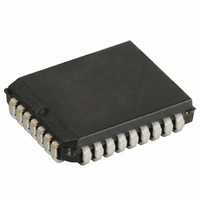
... Pin Configurations Figure 1. 32-Pin PLCC/LCC (Top View 323130 FL/ 7C421 XO/ 1617 181920 Document #: 38-06001 Rev. *F Figure 2. 28-Pin DIP (Top View FL/RT 0 7C420 7C424 MR 7C428 7C432 XO/ GND CY7C421 Figure 3. 32-PIn TQFP (Top View) 32 3130 FL/ 7C421 XO/ Page [+] Feedback ...
Page 5
... CC [ Max GND CC OUT –10 Test Conditions Min Max = Max., Commercial Industrial MAX = Max., Commercial Commercial 10 Min. Industrial Commercial 5 –0.2V Industrial CY7C421 [2] Ambient Temperature V CC 5V 10 5V 10% – +85 C All Speed Grades Min Max 2.4 0 [4] 0.8 – ...
Page 6
... Max., Commercial Industrial OUT MAX V = Max., Commercial OUT MHz All Inputs = Commercial V Min. Industrial IH All Inputs > Commercial V –0.2V Industrial CC Description Test Conditions Input Capacitance 4.5V Output Capacitance CC CY7C421 –40 –65 Max Min Max Min Max Max Unit MHz Page Unit ...
Page 7
... AC Test Load and Waveforms. HZR DVR Document #: 38-06001 Rev. *F –10 Min Max Min and –200 mV from transition is measured at the 1.5V level DVR CY7C421 –15 –20 –25 Max Min Max Min Max ...
Page 8
... Effective Write from Read HIGH WAF t Effective Write Pulse Width After FF HIGH WPF t Expansion Out LOW Delay from Clock XOL t Expansion Out HIGH Delay from Clock XOH Document #: 38-06001 Rev. *F –30 –40 Min Max Min Max Min CY7C421 –65 Unit Max Page [+] Feedback ...
Page 9
... Document #: 38-06001 Rev. *F Figure 4. Asynchronous Read and Write DVR DATA VALID DATA VALID DATA VALID Figure 5. Master Reset [11] t MRSC t PMR t RPW t WPW t t RMR EFL t HFH t FFH Figure 6. Half-full Flag HALF FULL+1 t WHF CY7C421 t HZR DATA VALID HALF FULL t RHF Page [+] Feedback ...
Page 10
... EF, HF and FF may change state during retransmit as a result of the offset of the read and write pointers, but flags are valid RTC PRT RTR Document #: 38-06001 Rev. *F ADDITIONAL FIRST READ READS t RFF ADDITIONAL FIRST WRITE WRITES t WEF [12] Figure 9. Retransmit [13] t RTC PRT t RTR CY7C421 FIRST WRITE FIRST READ VALID . RTC Page [+] Feedback ...
Page 11
... R EF DATA OUT Figure 11. Full Flag and Write Data Flow-through Mode DATA DATA OUT DATA VALID Document #: 38-06001 Rev RAE t RPE t REF t t WEF A t HWZ DATA VALID t t WAF WPF t t RFF WFF DATA VALID t SD CY7C421 t HD Page [+] Feedback ...
Page 12
... Expansion Out of device 1 ( connected to Expansion In of device 2 (XI 1 Document #: 38-06001 Rev. *F Figure 12. Expansion Timing Diagrams WRITE TO FIRST PHYSICAL LOCATION OF DEVICE XOH DATA VALID READ FROM FIRST PHYSICAL LOCATION OF DEVICE XOH t DVR DATA VALID CY7C421 DATA VALID t HZR t DVR DATA VALID Page [+] Feedback ...
Page 13
... Consequently, any depth or width FIFO can be created of word widths in increments of 9. When expanding in depth, a composite FF must be created by ORing the FFs together. Likewise, a composite EF is created by ORing the EFs together. HF and RT functions are not available in depth expansion mode. CY7C421 are in a high impedance condition 0 8 after a valid write ...
Page 14
... Figure 13. Depth Expansion CY7C420/1 CY7C424 CY7C428 CY7C432 CY7C420/1 CY7C424 CY7C428 CY7C432 CY7C420/1 CY7C424 CY7C428 CY7C432 FIRST DEVICE CY7C421 EMPTY Page [+] Feedback ...
Page 15
... Plastic Leaded Chip Carrier (Pb-free Temperature Range Commercial Industrial X = Pb-free (RoHS Compliant) Package Type 32-pin TQFP J = 32-pin PLCC V = 28-pin Molded SOJ Speed Depth: 512 2 = Width: × FIFO Technology Code CMOS 7 = Dual Port SRAM CY = Cypress Device CY7C421 Operating Range Commercial Commercial Industrial Page [+] Feedback ...
Page 16
... Package Diagrams Figure 14. 32-pin Thin Plastic Quad Flat Pack, 51-85063 Document #: 38-06001 Rev. *F CY7C421 51-85063 *C Page [+] Feedback ...
Page 17
... Figure 15. 32-pin Plastic Leaded Chip Carrier, 51-85002 Document #: 38-06001 Rev. *F CY7C421 51-85002 *C Page [+] Feedback ...
Page 18
... Document #: 38-06001 Rev. *F Figure 16. 28-pin (300-Mil) PDIP, 51-85014 CY7C421 51-85014 *E Page [+] Feedback ...
Page 19
... Figure 17. 28-pin (300-Mil) Molded SOJ, 51-85031 Document #: 38-06001 Rev. *F CY7C421 51-85031 *D Page [+] Feedback ...
Page 20
... Document History Page Document Title: CY7C421 256/512/1K/2K/4Kx9 Asynchronous FIFO Document Number: 38-06001 Orig. of Rev. ECN No. Change ** 106462 SZV *A 122332 RBI *B 383597 PCX *C 2623658 VKN/PYRS *D 2714768 VKN/AESA *E 2896039 RAME *F 3110157 ADMU Document #: 38-06001 Rev. *F Submission Description of Change Date 07/11/01 Change from Spec Number: 38-00079 to 38-06001 12/30/02 Added power up requirements to maximum ratings information ...
Page 21
... Cypress against all charges. Use may be limited by and subject to the applicable Cypress software license agreement. Document #: 38-06001 Rev. *F All products and company names mentioned in this document may be the trademarks of their respective holders. cypress.com/go/plc Revised December 14, 2010 CY7C421 PSoC Solutions psoc.cypress.com/solutions PSoC 1 | PSoC 3 ...