IDT72413L35P IDT, Integrated Device Technology Inc, IDT72413L35P Datasheet - Page 2
IDT72413L35P
Manufacturer Part Number
IDT72413L35P
Description
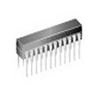
IC FIFO PAR W/FLAGS 32KB 20DIP
Manufacturer
IDT, Integrated Device Technology Inc
Series
7200r
Datasheet
1.IDT72413L25SO8.pdf
(10 pages)
Specifications of IDT72413L35P
Function
Asynchronous
Memory Size
32K
Access Time
35ns
Voltage - Supply
4.5 V ~ 5.5 V
Operating Temperature
0°C ~ 70°C
Mounting Type
Through Hole
Package / Case
20-DIP (0.300", 7.62mm)
Configuration
Dual
Density
320b
Access Time (max)
28.5(Min)ns
Word Size
5b
Organization
64x5
Sync/async
Asynchronous
Expandable
Yes
Bus Direction
Uni-Directional
Package Type
DIP
Clock Freq (max)
Not RequiredMHz
Operating Supply Voltage (typ)
5V
Operating Supply Voltage (min)
4.5V
Operating Supply Voltage (max)
5.5V
Supply Current
60mA
Operating Temp Range
0C to 70C
Operating Temperature Classification
Commercial
Mounting
Through Hole
Pin Count
20
Lead Free Status / RoHS Status
Contains lead / RoHS non-compliant
Data Rate
-
Lead Free Status / RoHS Status
Not Compliant, Contains lead / RoHS non-compliant
Other names
72413L35P
Available stocks
Company
Part Number
Manufacturer
Quantity
Price
Company:

Part Number:
IDT72413L35P
Manufacturer:
IDT
Quantity:
6 237


CAPACITANCE
(T
NOTE:
1. Characterized values, not currently tested.
PIN CONFIGURATION
DC ELECTRICAL CHARACTERISTICS
(Commercial: V
NOTES:
1. Care should be taken to minimize as much as possible the DC and capactive load on IR and OR when operating at frequencies above 25MHz.
2. Not more than one output should be shorted at a time and duration of the short circuit should not exceed one second. Guaranteed by design, but not currently tested.
3. Tested with outputs open (I
4. For frequencies greater than 25MHz, I
IDT72413 CMOS PARALLEL FIFO WITH FLAGS
64 x 5
Symbol
A
Symbol
C
C
I
V
V
I
I
I
I
IIH
OS
CC
IL
HZ
L Z
= +25°C, f = 1.0MHz)
I N
OUT
O L
OH
(3,4)
(2)
GND
Low-Level Input Current
Low-Level Output Current
High-Level Output Current
Output Short-Circuit Current
HIGH Impedance Output Current
LOW Impedance Output Current
Active Supply Current
OE
HF
D
D
D
D
D
High-Level Input Current
IR
SI
PLASTIC DIP (P20-1, ORDER CODE: P)
Input Capacitance
Output Capacitance
CC
0
1
2
3
4
SOIC (SO20-2, ORDER CODE: SO)
Parameter
= 5.0V ± 10%, T
10
1
2
3
4
5
6
7
8
9
Parameter
OUT
= 0).
TOP VIEW
CC
A
= 0°C to +70°C)
= 60mA + (1.5mA x [f –25MHz]) commercial.
V
V
Conditions
IN
OUT
20
19
18
17
16
15
14
13
12
11
= 0V
= 0V
2748 drw 02
V
V
V
V
V
V
V
Inputs LOW, f = 25MHz
OR
MR
Vcc
AF/E
SO
Q
Q
Q
Q
Q
V
CC
CC
CC
CC
CC
CC
CC
CC
0
1
2
3
4
= Min.
= Min.
= Max., GND ≤ V
= Max. V
= Max. V
= Max. V
= Max., OE = HIGH
= Max., GND ≤ V
Max.
5
7
Test Conditions
I
I
I
I
I
I
2748 tbl 02
OL
OL
OL
OH
OH
OH
O
O
O
Unit
pF
pF
(Q
(IR, OR)
= 0V
= 2.4V
= 0.4V
(HF, AF/E)
(IR, OR)
(HF, AF/E)
(Q
0-4
0-4
I
2
≤ V
)
I
)
≤ V
NOTE:
1. Stresses greater than those listed under ABSOLUTE MAXIMUM RATINGS may
ABSOLUTE MAXIMUM RATINGS
RECOMMENDED OPERATING
CONDITIONS
NOTE:
1. 1.5V undershoots are allowed for 10ns once per cycle.
CC
(1)
V
T
I
cause permanent damage to the device. This is a stress rating only and
functional operation of the device at these or any other conditions above those
indicated in the operational sections of this specification is not implied. Exposure
to absolute maximum rating conditions for extended periods may affect reliability.
Symbol
OUT
CC
STG
V
GND
V
V
T
TERM
A
CC
IL
IH
Symbol
(1)
24 mA
–4mA
–4mA
–4mA
8mA
8mA
Supply Voltage
Commercial
Supply Voltage
Input High Voltage
Input Low Voltage
Operating Temperature
Commercial
Terminal Voltage with
Respect to GND
Storage
Temperature
DC Output
Current
Parameter
Min.
Rating
–10
–20
–20
2.4
—
—
—
—
COMMERCIAL TEMPERATURE RANGE
f
IN
= 45, 35, 25 MHz
Commercial
IDT72413
Min.
4.5
2.0
—
0
0
–0.5 to +7.0
Commercial
–55 to +125
–50 to +50
Max.
–110
0.4
Typ.
20
60
—
—
—
5.0
10
—
—
—
0
Max.
(1)
5.5
0.8
70
—
0
m A
Unit
° C
Unit
V
µ A
m A
µ A
µ A
m A
µ A
Unit
V
V
° C
V
V
V
V
Related parts for IDT72413L35P
Image
Part Number
Description
Manufacturer
Datasheet
Request
R

Part Number:
Description:
TRANSLATION DEVICE DPI 80-PQFP
Manufacturer:
IDT, Integrated Device Technology Inc
Datasheet:
Part Number:
Description:
IDT PART
Manufacturer:
IDT, Integrated Device Technology Inc
Datasheet:
Part Number:
Description:
IC LIU T1/E1/J1 OCTAL 256PBGA
Manufacturer:
IDT, Integrated Device Technology Inc
Datasheet:

Part Number:
Description:
IC FREQ TIMING GENERATOR 28TSSOP
Manufacturer:
IDT, Integrated Device Technology Inc
Datasheet:
Part Number:
Description:
IC CLK DVR PLL 1:10 40VFQFPN
Manufacturer:
IDT, Integrated Device Technology Inc
Datasheet:
Part Number:
Description:
IC CLK FANOUT BUFFER 1:18 32LQFP
Manufacturer:
IDT, Integrated Device Technology Inc
Datasheet:
Part Number:
Description:
IC CLK FANOUT BUFFER 1:18 32LQFP
Manufacturer:
IDT, Integrated Device Technology Inc
Datasheet:
Part Number:
Description:
IC CK505 VREG/RES 56TSSOP
Manufacturer:
IDT, Integrated Device Technology Inc
Datasheet:

Part Number:
Description:
IC SDRAM CLK DVR 1:10 48-TSSOP
Manufacturer:
IDT, Integrated Device Technology Inc
Datasheet:

Part Number:
Description:
IC CLK DVR PLL 1:10 48TSSOP
Manufacturer:
IDT, Integrated Device Technology Inc
Datasheet:
Part Number:
Description:
IC FLEXPC CLK PROGR P4 56-TSSOP
Manufacturer:
IDT, Integrated Device Technology Inc
Datasheet:
Part Number:
Description:
IC FLEXPC CLK PROGR P4 56-TSSOP
Manufacturer:
IDT, Integrated Device Technology Inc
Datasheet:
Part Number:
Description:
IC FLEXPC CLK PROGR P4 56-SSOP
Manufacturer:
IDT, Integrated Device Technology Inc
Datasheet:

Part Number:
Description:
IC PLL CLK DRIVER 2.5V 28-TSSOP
Manufacturer:
IDT, Integrated Device Technology Inc
Datasheet:
Part Number:
Description:
IC CLOCK DRIVER 2.5V 24-TSSOP
Manufacturer:
IDT, Integrated Device Technology Inc
Datasheet: