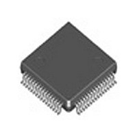
IDT72V275L20TF IDT, Integrated Device Technology Inc, IDT72V275L20TF Datasheet - Page 2

IDT72V275L20TF
Manufacturer Part Number
IDT72V275L20TF
Description
IC FIFO SS 32768X18 20NS 64STQFP
Manufacturer
IDT, Integrated Device Technology Inc
Series
72Vr
Datasheet
1.IDT72V275L15TF8.pdf
(25 pages)
Specifications of IDT72V275L20TF
Function
Synchronous
Memory Size
589K (32K x 18)
Access Time
20ns
Voltage - Supply
3 V ~ 3.6 V
Operating Temperature
0°C ~ 70°C
Mounting Type
Surface Mount
Package / Case
64-STQFP
Configuration
Dual
Density
576Kb
Access Time (max)
12ns
Word Size
18b
Organization
32Kx18
Sync/async
Synchronous
Expandable
Yes
Bus Direction
Uni-Directional
Package Type
STQFP
Clock Freq (max)
50MHz
Operating Supply Voltage (typ)
3.3V
Operating Supply Voltage (min)
3V
Operating Supply Voltage (max)
3.6V
Supply Current
60mA
Operating Temp Range
0C to 70C
Operating Temperature Classification
Commercial
Mounting
Surface Mount
Pin Count
64
Lead Free Status / RoHS Status
Contains lead / RoHS non-compliant
Data Rate
-
Lead Free Status / Rohs Status
Not Compliant
Other names
72V275L20TF
Available stocks
Company
Part Number
Manufacturer
Quantity
Price
Company:
Part Number:
IDT72V275L20TF
Manufacturer:
IDT, Integrated Device Technology Inc
Quantity:
10 000
Company:
Part Number:
IDT72V275L20TF8
Manufacturer:
IDT, Integrated Device Technology Inc
Quantity:
10 000
DESCRIPTION (Continued)
PIN CONFIGURATIONS
(WEN) input. Data is written into the FIFO on every rising edge of WCLK when
WEN is asserted. The output port is controlled by a Read Clock (RCLK) input
and Read Enable (REN) input. Data is read from the FIFO on every rising
edge of RCLK when REN is asserted. An Output Enable (OE) input is provided
for three-state control of the outputs.
to f
of the one clock input with respect to the other.
Standard mode and First Word Fall Through (FWFT) mode.
NOTE:
1. DC = Don’t Care. Must be tied to GND or V
IDT72V275/72V285 3.3V CMOS SUPERSYNC FIFO
32,768 x 18 and 65,536 x 18
MAX
The input port is controlled by a Write Clock (WCLK) input and a Write Enable
The frequencies of both the RCLK and the WCLK signals may vary from 0
There are two possible timing modes of operation with these devices: IDT
with complete independence. There are no restrictions on the frequency
PIN 1
DC
WEN
GND
SEN
D17
D16
D15
D14
D13
D12
D11
D10
V
D9
D8
D7
CC
(1)
1
2
3
4
5
6
7
8
9
10
11
12
13
14
15
16
CC
, cannot be left open.
64 63 62 61 60 59 58 57 56 55 54 53 52 51 50 49
17 18 19 20 21 22 23 24 25 26 27 28 29 30 31 32
TM
STQFP (PP64-1, order code: TF)
TQFP (PN64-1, order code: PF)
TOP VIEW
2
on the data output lines unless a specific read operation is performed. A read
operation, which consists of activating REN and enabling a rising RCLK edge,
will shift the word from internal memory to the data output lines.
to the data output lines after three transitions of the RCLK signal. A REN does
not have to be asserted for accessing the first word. However, subsequent
words written to the FIFO do require a LOW on REN for access. The state of
the FWFT/SI input during Master Reset determines the timing mode in use.
can provide, the FWFT timing mode permits depth expansion by chaining FIFOs
in series (i.e. the data outputs of one FIFO are connected to the corresponding
data inputs of the next). No external logic is required.
In IDT Standard mode, the first word written to an empty FIFO will not appear
In FWFT mode, the first word written to an empty FIFO is clocked directly
For applications requiring more data storage capacity than a single FIFO
48
47
46
45
44
43
42
41
40
39
38
37
36
35
34
33
COMMERCIAL AND INDUSTRIAL
4512 drw 02
TEMPERATURE RANGES
Q17
Q16
GND
Q15
Q14
V
Q13
Q12
Q11
GND
Q10
Q9
Q8
Q7
Q6
GND
CC


