CY7C419-10JXCT Cypress Semiconductor Corp, CY7C419-10JXCT Datasheet
CY7C419-10JXCT
Specifications of CY7C419-10JXCT
Available stocks


Related parts for CY7C419-10JXCT


CY7C419-10JXCT Summary of contents
Page 1
... FIFOs to retransmit the data. Read enable (R) and write enable (W) must both be HIGH during retransmit, and then R is used to access the data. The CY7C419, CY7C420, CY7C421, CY7C424, CY7C425, CY7C428, CY7C429, CY7C432, and CY7C433 are fabricated using an advanced 0.65-micron P-well CMOS technology. Input ESD protection is greater than 2000V and latch-up is prevented by careful layout and guard rings ...
Page 2
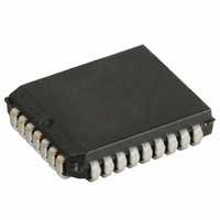
... Pin Configurations Figure 1. 32-Pin PLCC/LCC Figure 2. 28-Pin DIP Table 1. Selection Guide –10 Frequency (MHz) 50 Maximum Access Time (ns (mA) 35 CC1 Document #: 38-06001 Rev. *C Figure 3. 32-PIn TQFP –15 –20 –25 –30 40 33.3 28 CY7C419/21/25/29/33 –40 – 12 Page [+] Feedback ...
Page 3
... Range Commercial Industrial [3] Test Conditions V = Min –2 Min 8 Commercial Industrial GND < V < > GND < V < [ Max GND CC OUT CY7C419/21/25/29/33 [2] Ambient Temperature V CC ° ° 5V ± 10 ° ° 5V ± 10% – +85 C All Speed Grades Unit Min Max 2.4 V 0 [4] 0.8 V μ ...
Page 4
... Industrial [3] –30 Test Conditions Min Max = Max., Commercial Industrial 75 MAX = Max., Commercial Commercial 10 Min. Industrial 15 Commercial 5 –0.2V Industrial 8 Description Test Conditions ° MHz 4.5V CC CY7C419/21/25/29/33 –15 –20 –25 Min Max Min Max Min Max 100 –40 –65 Unit Min Max Min ...
Page 5
... AC Test Load and Waveforms. HZR DVR Document #: 38-06001 Rev. *C [7, 8] –10 –15 Min Max Min and –200 mV from transition is measured at the 1.5V level DVR CY7C419/21/25/29/33 –20 –25 Unit Max Min Max Min Max ...
Page 6
... Effective Write from Read HIGH WAF t Effective Write Pulse Width After FF HIGH WPF t Expansion Out LOW Delay from Clock XOL t Expansion Out HIGH Delay from Clock XOH Document #: 38-06001 Rev. *C CY7C419/21/25/29/33 [7, 8] (continued) –30 –40 Min Max Min Max Min 40 50 ...
Page 7
... Document #: 38-06001 Rev. *C Figure 4. Asynchronous Read and Write DVR DATA VALID DATA VALID DATA VALID Figure 5. Master Reset [12] t MRSC t PMR t RPW t WPW t t RMR EFL t HFH t FFH Figure 6. Half-full Flag HALF FULL+1 t WHF CY7C419/21/25/29/33 t HZR DATA VALID HALF FULL t RHF Page [+] Feedback ...
Page 8
... EF, HF and FF may change state during retransmit as a result of the offset of the read and write pointers, but flags will be valid RTC PRT RTR Document #: 38-06001 Rev. *C ADDITIONAL FIRST READ READS t RFF ADDITIONAL FIRST WRITE WRITES t WEF [13] Figure 9. Retransmit [14] t RTC PRT t RTR CY7C419/21/25/29/33 FIRST WRITE FIRST READ VALID . RTC Page [+] Feedback ...
Page 9
... Figure 10. Empty Flag and Read Data Flow-through Mode DATA DATA OUT Figure 11. Full Flag and Write Data Flow-through Mode DATA DATA OUT DATA VALID Document #: 38-06001 Rev RAE t RPE t REF t t WEF A t HWZ DATA VALID t t WAF WPF t t RFF WFF DATA VALID t SD CY7C419/21/25/29/ Page [+] Feedback ...
Page 10
... Expansion Out of device 1 ( connected to Expansion In of device 2 (XI 1 Document #: 38-06001 Rev. *C Figure 12. Expansion Timing Diagrams WRITE TO FIRST PHYSICAL LOCATION OF DEVICE XOH DATA VALID READ FROM FIRST PHYSICAL LOCATION OF DEVICE XOH t DVR DATA VALID CY7C419/21/25/29/ DATA VALID t HZR t DVR DATA VALID Page [+] Feedback ...
Page 11
... FIFO and the full flag must be used to prevent writing into a full FIFO. For example, consider an empty FIFO that is receiving read pulses. Because the FIFO is empty, the read pulses are ignored by the FIFO, and nothing happens. Next, a single word is written CY7C419/21/25/29/33 after RTR . FIFOs can be CC ...
Page 12
... Figure 13. Depth Expansion CY7C419 9 CY7C420/1 CY7C424/5 CY7C428/9 CY7C432 CY7C419 9 CY7C420/1 CY7C424/5 CY7C428/9 CY7C432 CY7C419 9 CY7C420/1 CY7C424/5 CY7C428/9 CY7C432 FIRST DEVICE CY7C419/21/25/29/ EMPTY Page [+] Feedback ...
Page 13
... Molded SOJ J65 32-Pin Plastic Leaded Chip Carrier J65 32-Pin Plastic Leaded Chip Carrier P21 28-Pin (300-Mil) Molded DIP V21 28-Pin (300-Mil) Molded SOJ J65 32-Pin Plastic Leaded Chip Carrier CY7C419/21/25/29/33 Operating Range Commercial Commercial Industrial Commercial Industrial Commercial Industrial Commercial ...
Page 14
... Package Diagrams Figure 14. 32-Pin Thin Plastic Quad Flat Pack A32 (51-85063) Figure 15. 32-Pin Plastic Leaded Chip Carrier J65 (51-85002) Document #: 38-06001 Rev. *C CY7C419/21/25/29/33 51-85063-*B 51-85002-*B Page [+] Feedback ...
Page 15
... SEATING PLANE 0.120[3.05] 0.140[3.55] 0.009[0.23] 0.012[0.30] 0.015[0.38] 0.060[1.52] 0.055[1.39] 0.065[1.65] 0.015[0.38] 0.020[0.50] SEE LEAD END OPTION CY7C419/21/25/29/33 DIMENSIONS IN INCHES [MM] MIN. MAX. REFERENCE JEDEC MO-095 PACKAGE WEIGHT: 2.15 gms 0.290[7.36] 0.325[8.25] 3° MIN. 0.310[7.87] 0.385[9.78] 51-85014-*D Page [+] Feedback ...
Page 16
... Package Diagrams (continued) Figure 17. 28-Pin (300-Mil) Molded SOJ V21(51-85031) Document #: 38-06001 Rev. *C CY7C419/21/25/29/33 51-85031-*C Page [+] Feedback ...
Page 17
... Document History Page Document Title: CY7C419, CY7C421, CY7C425, CY7C429, CY7C433, 256/512/1K/2K/4Kx9 Asynchronous FIFO Document Number: 38-06001 Orig. of Rev. ECN No. Change ** 106462 SZV *A 122332 RBI *B 383597 PCX *C 2623658 VKN/PYRS Sales, Solutions and Legal Information Worldwide Sales and Design Support Cypress maintains a worldwide network of offices, solution centers, manufacturer’s representatives, and distributors. To find the office closest to you, visit us at cypress ...