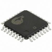
CY7C4211-10AXI Cypress Semiconductor Corp, CY7C4211-10AXI Datasheet - Page 12

CY7C4211-10AXI
Manufacturer Part Number
CY7C4211-10AXI
Description
IC SYNC FIFO MEM 512X9 32-TQFP
Manufacturer
Cypress Semiconductor Corp
Series
CY7Cr
Specifications of CY7C4211-10AXI
Function
Synchronous
Memory Size
4.6K (512 x 9)
Data Rate
100MHz
Access Time
8ns
Voltage - Supply
3.3V
Operating Temperature
-40°C ~ 85°C
Mounting Type
Surface Mount
Package / Case
32-TQFP
Configuration
Dual
Density
4Kb
Access Time (max)
8ns
Word Size
9b
Organization
512x9
Sync/async
Synchronous
Expandable
Yes
Bus Direction
Uni-Directional
Clock Freq (max)
100MHz
Operating Supply Voltage (typ)
5V
Operating Supply Voltage (min)
4.5V
Operating Supply Voltage (max)
5.5V
Supply Current
40mA
Operating Temp Range
-40C to 85C
Operating Temperature Classification
Industrial
Mounting
Surface Mount
Pin Count
32
Lead Free Status / RoHS Status
Lead free / RoHS Compliant
Available stocks
Company
Part Number
Manufacturer
Quantity
Price
Company:
Part Number:
CY7C4211-10AXI
Manufacturer:
Cypress Semiconductor Corp
Quantity:
10 000
Company:
Part Number:
CY7C4211-10AXIT
Manufacturer:
Cypress Semiconductor Corp
Quantity:
10 000
Document #: 38-06016 Rev. *B
Switching Waveforms
Notes:
Programmable Almost Full Flag Timing
Write Programmable Registers
22. t
23. PAE offset = n.
24. If a Read is performed on this rising edge of the Read clock, there will be Empty + (n – 1) words in the FIFO when PAE goes LOW.
25. If a Write is performed on this rising edge of the Write clock, there will be Full – (m – 1) words of the FIFO when PAF goes LOW.
26. PAF offset = m.
27. 64-m words for CY7C4421, 256 – m words in FIFO for CY7C4201, 512 – m words for CY7C4211, 1024 – m words for CY7C4221, 2048 – m words for CY7C4231,
28. t
(if applicable)
WEN2/LD
WEN2
WCLK and the rising RCLK is less than t
4096 – m words for CY7C4241, 8192 – m words for CY7C4251.
edge of RCLK and the rising edge of WCLK is less than t
SKEW2
SKEW2
WEN1
WCLK
WCLK
D
WEN1
REN1,
RCLK
REN2
0
PAF
–D
is the minimum time between a rising WCLK and a rising RCLK edge for PAE to change state during that clock cycle. If the time between the edge of
is the minimum time between a rising RCLK edge and a rising WCLK edge for PAF to change during that clock cycle. If the time between the rising
8
t
t
CLKH
CLKH
FULL
(continued)
t
CLK
t
t
ENS
ENS
t
IN FIFO
DS
SKEW2
M+1 WORDS
PAE OFFSET
t
t
ENS
ENS
, then PAE may not change state until the next RCLK.
LSB
t
t
ENH
ENH
t
t
CLKL
CLKL
SKEW2
t
ENH
t
DH
, then PAF may not change state until the next WCLK.
Note
PAE OFFSET
26
Note
25
MSB
t
PAF
t
ENS
PAF OFFSET
t
SKEW2
FULL
CY7C4421/4201/4211/4221
LSB
IN FIFO
t
[28]
ENS
M WORDS
CY7C4231/4241/4251
t
[27]
ENH
PAF OFFSET
MSB
t
PAF
Page 12 of 18


