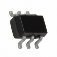
NC7SZ374P6X Fairchild Semiconductor, NC7SZ374P6X Datasheet - Page 4

NC7SZ374P6X
Manufacturer Part Number
NC7SZ374P6X
Description
IC FLIP FLOP DTYPE TRI-ST SC70-6
Manufacturer
Fairchild Semiconductor
Series
7SZr
Type
D-Typer
Datasheet
1.NC7SZ374P6X.pdf
(9 pages)
Specifications of NC7SZ374P6X
Function
Standard
Output Type
Tri-State Non Inverted
Number Of Elements
1
Number Of Bits Per Element
1
Frequency - Clock
100MHz
Delay Time - Propagation
9.7ns
Trigger Type
Positive Edge
Current - Output High, Low
32mA, 32mA
Voltage - Supply
1.65 V ~ 5.5 V
Operating Temperature
-40°C ~ 85°C
Mounting Type
Surface Mount
Package / Case
SC-70-6, SC-88, SOT-363
Number Of Circuits
1
Logic Family
74P
Logic Type
D-Type Flip-Flop
Polarity
Non-Inverting
Input Type
Single-Ended
Propagation Delay Time
5.5 ns
High Level Output Current
- 32 mA
Low Level Output Current
32 mA
Supply Voltage (max)
5.5 V
Maximum Operating Temperature
+ 85 C
Mounting Style
SMD/SMT
Minimum Operating Temperature
- 40 C
Supply Voltage (min)
1.65 V
Technology
CMOS
Number Of Bits
1
Number Of Elements
1
Clock-edge Trigger Type
Positive-Edge
Operating Supply Voltage (typ)
1.8/2.5/3.3/5V
Package Type
SC-70
Frequency (max)
175MHz
Operating Supply Voltage (min)
1.65V
Operating Supply Voltage (max)
5.5V
Operating Temp Range
-40C to 85C
Operating Temperature Classification
Industrial
Mounting
Surface Mount
Pin Count
6
Lead Free Status / RoHS Status
Lead free / RoHS Compliant
Other names
NC7SZ374P6XTR
Available stocks
Company
Part Number
Manufacturer
Quantity
Price
Company:
Part Number:
NC7SZ374P6X
Manufacturer:
FSC
Quantity:
69 000
Part Number:
NC7SZ374P6X
Manufacturer:
FAIRCHILD/ن»™ç«¥
Quantity:
20 000
www.fairchildsemi.com
C
C
C
f
t
t
t
t
t
t
t
t
t
MAX
PLH
PHL
PZL
PZH
PLZ
PHZ
S
H
W
Symbol
AC Electrical Characteristics
Capacitance
Note 3: T
Note 4: C
loading and operating at 50% duty cycle. (See Figure 2) C
I
IN
OUT
PD
CCD
Symbol
(C
PD
A
PD
Maximum Clock
Frequency
Propagation Delay
CP to Q
Output Enable Time
Output Disable Time
Setup Time,
CP to D
Hold Time,
CP to D
Pulse Width, CP
) (V
is defined as the value of the internal equivalent capacitance which is derived from dynamic operating current consumption (I
25C, f
CC
) (f
Parameter
Input Capacitance
Output Capacitance
Power Dissipation Capacitance (Note 4)
IN
)
1MHz.
(I
CC
(Note 3)
static).
2.5
3.3
5.0
2.5
3.3
5.0
3.3
5.0
2.5
3.3
5.0
2.5
3.3
5.0
2.5
3.3
5.0
3.3
5.0
2.5
3.3
5.0
2.5
1.65
1.65
1.65
1.65
V
1.8
1.8
1.8
1.8
(V)
CC
Parameter
0.2
0.3
0.5
0.2
0.3
0.5
0.3
0.5
0.2
0.3
0.5
0.2
0.3
0.5
0.2
0.3
0.5
0.2
0.3
0.5
0.2
0.3
0.5
Min
2.5
2.5
2.0
1.5
1.0
2.0
1.5
2.0
2.0
2.0
1.5
1.0
2.0
2.0
2.0
1.5
1.0
PD
is related to I
T
A
Typ
9.7
6.5
3.8
2.8
2.2
3.4
2.6
9.0
6.0
3.7
2.8
2.2
7.7
5.1
3.5
2.8
2.3
25 C
CCD
Max
1.50
10.0
13.5
12.0
4
6.5
4.5
3.5
5.5
4.0
9.0
6.0
5.0
3.7
8.0
6.0
4.5
3.7
dynamic operating current by the expression:
Typ
10
12
3
4
T
A
Min
100
100
125
150
175
2.5
2.5
2.0
1.4
1.0
1.6
1.4
2.0
2.0
1.8
1.4
1.0
2.0
2.0
1.8
1.4
1.0
2.5
2.0
1.5
1.5
1.5
1.5
3.0
2.8
2.5
40 C to 85 C
Max
Max
16.5
11.0
14.3
13.0
7.0
5.0
3.8
6.2
4.7
9.5
6.6
5.3
3.9
8.5
6.3
4.7
3.9
Units
pF
pF
pF
Units
MHz
ns
ns
ns
ns
ns
ns
V
V
V
V
CC
CC
CC
CC
C
R
C
R
S
C
R
C
R
S1
S1
C
R
S1
S1
C
R
C
D
CL
R
Open, V
3.3V, V
3.3V
5.0V
1
L
D
L
D
L
D
L
U
L
U
L
D
L
D
, R
, R
500 , S
Open
50 pF
15 pF
50 pF
50 pF, V
50 pF, V
50 pF
50 pF
500 , S
1 M
500 , S
GND for t
V
GND for t
V
500 , S
50 pF
500 , S
D
D
Conditions
I
I
for t
for t
IN
Conditions
IN
500
500
PZL
PLZ
0V or V
1
0V or V
I
I
1
1
1
1
PZH
PHZ
CCD
Open
2x V
2x V
Open
Open
Open
Open
) at no output
CC
CC
CC
CC
Number
Figures
Figures
Figures
Figures
Figures
Figures
Figures
Figures
Figure
1, 3
1, 3
1, 3
1, 4
1, 4
1, 5
1, 5
1, 5


