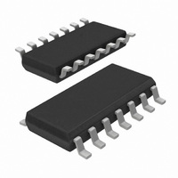
74LVC74AD,118 NXP Semiconductors, 74LVC74AD,118 Datasheet - Page 6

74LVC74AD,118
Manufacturer Part Number
74LVC74AD,118
Description
IC DUAL D-TYPE FLIP-FLOP 14-SOIC
Manufacturer
NXP Semiconductors
Series
74LVCr
Type
D-Typer
Datasheet
1.74LVC74AD118.pdf
(16 pages)
Specifications of 74LVC74AD,118
Package / Case
14-SOIC (3.9mm Width), 14-SOL
Function
Set(Preset) and Reset
Output Type
Differential
Number Of Elements
2
Number Of Bits Per Element
1
Frequency - Clock
250MHz
Trigger Type
Positive Edge
Current - Output High, Low
24mA, 24mA
Voltage - Supply
2.7 V ~ 3.6 V
Operating Temperature
-40°C ~ 125°C
Mounting Type
Surface Mount
Number Of Circuits
2
Logic Family
74LVC
Logic Type
D-Type Flip-Flop
Polarity
Inverting/Non-Inverting
Input Type
Single-Ended
Propagation Delay Time
7 ns
High Level Output Current
- 24 mA
Supply Voltage (max)
3.6 V
Maximum Operating Temperature
+ 125 C
Mounting Style
SMD/SMT
Minimum Operating Temperature
- 40 C
Supply Voltage (min)
1.2 V
Technology
CMOS
Number Of Bits
2
Number Of Elements
2
Clock-edge Trigger Type
Positive-Edge
Operating Supply Voltage (typ)
1.8/2.5/3.3V
Package Type
SO
Low Level Output Current
24mA
Frequency (max)
120MHz
Operating Supply Voltage (min)
1.2V
Operating Supply Voltage (max)
3.6V
Operating Temp Range
-40C to 125C
Operating Temperature Classification
Automotive
Mounting
Surface Mount
Pin Count
14
Lead Free Status / RoHS Status
Lead free / RoHS Compliant
Delay Time - Propagation
-
Lead Free Status / Rohs Status
Lead free / RoHS Compliant
Other names
568-2305-2
74LVC74AD-T
935260734118
74LVC74AD-T
935260734118
NXP Semiconductors
10. Dynamic characteristics
Table 8.
Voltages are referenced to GND (ground = 0 V). For test circuit see
[1]
[2]
[3]
74LVC74A_6
Product data sheet
Symbol Parameter
t
t
t
t
t
f
t
C
pd
W
rec
su
h
max
sk(o)
PD
Typical values are measured at T
t
Skew between any two outputs of the same package switching in the same direction. This parameter is guaranteed by design.
pd
is the same as t
propagation
delay
pulse width
recovery time
set-up time
hold time
maximum
frequency
output skew time V
power
dissipation
capacitance
Dynamic characteristics
PLH
and t
Conditions
nCP to nQ, nQ; see
nSD to nQ, nQ; see
nRD to nQ, nQ; see
clock HIGH or LOW; see
set or reset LOW; see
set or reset; see
nD to nCP; see
nD to nCP; see
nCP; see
per flip-flop; V
PHL
CC
V
V
V
V
V
V
V
V
V
V
V
V
V
V
V
V
V
V
V
V
V
V
.
CC
CC
CC
CC
CC
CC
CC
CC
CC
CC
CC
CC
CC
CC
CC
CC
CC
CC
CC
CC
CC
CC
= 3.0 V to 3.6 V
amb
= 1.2 V
= 2.7 V
= 3.0 V to 3.6 V
= 1.2 V
= 2.7 V
= 3.0 V to 3.6 V
= 1.2 V
= 2.7 V
= 3.0 V to 3.6 V
= 2.7 V
= 3.0 V to 3.6 V
= 2.7 V
= 3.0 V to 3.6 V
= 2.7 V
= 3.0 V to 3.6 V
= 2.7 V
= 3.0 V to 3.6 V
= 2.7 V
= 3.0 V to 3.6 V
= 2.7 V
= 3.0 V to 3.6 V
= 3.3 V
= 25 C. For V
Figure 7
I
= GND to V
Figure 7
Figure 7
Figure 8
Figure 7
Figure 8
Figure 8
CC
Rev. 06 — 4 June 2007
Figure 8
Dual D-type flip-flop with set and reset; positive-edge trigger
= 3.0 V to 3.6 V range, typical values are measured at 3.3 V.
Figure 7
CC
[2]
[3]
[4]
Figure
+1.0
+1.0
Min
150
1.0
1.0
1.0
1.0
1.0
1.0
3.3
3.3
3.3
3.3
1.5
2.2
2.0
1.0
83
-
-
-
-
-
9.
40 C to +85 C
Typ
250
2.7
2.5
3.2
2.5
3.2
2.5
1.3
1.7
0.8
15
15
15
15
3.0
0.2
-
-
-
-
-
-
-
[1]
Max
6.0
5.2
6.4
5.4
6.4
5.4
1.0
-
-
-
-
-
-
-
-
-
-
-
-
-
-
-
40 C to +125 C Unit
Min
120
1.0
1.0
1.0
1.0
1.0
1.0
4.5
4.5
4.5
4.5
1.0
1.0
2.2
2.0
1.0
1.0
66
74LVC74A
-
-
-
-
-
© NXP B.V. 2007. All rights reserved.
Max
7.5
6.5
8.0
7.0
8.0
7.0
1.5
-
-
-
-
-
-
-
-
-
-
-
-
-
-
-
-
ns
ns
ns
ns
ns
ns
ns
ns
ns
ns
ns
ns
ns
ns
ns
ns
ns
ns
ns
MHz
MHz
ns
pF
6 of 16


