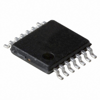
74LVT74PW,112 NXP Semiconductors, 74LVT74PW,112 Datasheet - Page 4

74LVT74PW,112
Manufacturer Part Number
74LVT74PW,112
Description
IC DUAL D-TYPE F-F 3.3V 14-TSSOP
Manufacturer
NXP Semiconductors
Series
74LVTr
Type
D-Typer
Datasheet
1.74LVT74D118.pdf
(10 pages)
Specifications of 74LVT74PW,112
Function
Set(Preset) and Reset
Output Type
Differential
Number Of Elements
2
Number Of Bits Per Element
1
Frequency - Clock
345MHz
Delay Time - Propagation
3.1ns
Trigger Type
Positive Edge
Current - Output High, Low
20mA, 32mA
Voltage - Supply
2.7 V ~ 3.6 V
Operating Temperature
-40°C ~ 85°C
Mounting Type
Surface Mount
Package / Case
14-TSSOP
Lead Free Status / RoHS Status
Lead free / RoHS Compliant
Other names
568-3050-5
935209270112
935209270112
1. All typical values are at V
2. This is the increase in supply current for each input at the specificed voltage level other than V
1. All typical values are at V
Philips Semiconductors
DC ELECTRICAL CHARACTERISTICS
Over recommended operating conditions
Voltages are referenced to GND (ground = 0V)
NOTES:
AC CHARACTERISTICS
GND = 0V; t
NOTE:
AC SETUP REQUIREMENTS
1996 Aug 28
SYMBOL
SYMBOL
3.3V Dual D-type flip-flop
SYMBOL
V
I
V
V
I
OFF
CC
C
f
t
I
t
t
t
t
t
t
t
t
t
OH
OL
I
I
t
W
CC
MAX
W
W
IK
PLH
PHL
PLH
PHL
S
h
I
I
S
h
t
I
rec
(H)
(H)
(L)
(L)
(H)
(L)
(L)
R
= t
Input clamp voltage
High-level output voltage
Low-level output voltage
Input leakage current
In ut leakage current
Output off current
Quiescent supply current
Additional supply current per input pin
Input capacitance
F
Maximum clock frequency
Propagation delay
CPn to Qn or Qn
Propagation delay
SDn, RDn to Qn or Qn
= 2.5ns; C
Setup time
Dn to CPn
Holdtime
Dn to CPn
CPn Pulse Width
SDn, RDn Pulse Width
Recovery time
SDn, RDn tp CPn
CC
CC
PARAMETER
L
PARAMETER
= 50pF, R
= 3.3V and T
= 3.3V and T
PARAMETER
L
= 500 ; T
amb
amb
= 25 C.
= 25 C.
amb
2
= –40 C to +85 C.
V
V
V
V
V
V
V
V
V
V
V
V
V
Other inputs at V
V
CC
CC
CC
CC
CC
CC
CC
CC
CC
CC
CC
CC,
CC
I
= 3V or 0
WAVEFORM
= 2.7V; I
= 2.7 to 3.6V; I
= 2.7V; I
= 3.0V; I
= 2.7V; I
= 2.7V; I
= 3.0V; I
= 0 or 3.6V; V
= 3.6V; V
= 0V; V
= 3.6V; Outputs High, V
= 3V to 3.6V; One input at V
I
O =
0
1
1
2
WAVEFORM
4
TEST CONDITIONS
I
IK
OH
OH
OL
OL
OL
or V
I
= V
= –18mA
1
1
1
2
3
= 100 A
= 24mA
= 32mA
= –6mA
= –20mA
CC
O
I
CC
OH
= 0 to 4.5V
= 5.5V
or GND
or GND
= –100 A
MIN
150
1.0
1.0
1.0
1.0
I
= GND or
V
CC
CC
V
MIN
CC
1.7
1.4
0.3
2.0
2.0
2.0
0.5
–0.6V,
= 3.3V
0
CC
TYP
345
= 3.3V
3.1
3.6
3.1
3.0
or GND.
1
LIMITS
0.3V
V
TYP
–0.3
–0.6
–0.3
LIMITS
0.3V
0.6
0.4
1.0
1.2
1.0
Temp = -40 C to +85 C
CC
MIN
MAX
2.4
2.0
4.8
5.0
5.0
4.4
–0.2
LIMITS
V
TYP
V
CC
0.5
3
CC
MIN
1.8
1.6
0.3
3.0
3.0
3.0
0.5
MAX
= 2.7V
Product specification
1
0
5.8
5.0
6.2
4.8
= 2.7V
74LVT74
MAX
–1.2
0.2
0.5
0.5
0.2
10
100
1
1
UNIT
UNIT
MHz
UNIT
ns
ns
ns
ns
ns
ns
mA
pF
V
V
V
A
A
A
A


