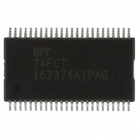
IDT74FCT162374ATPAG IDT, Integrated Device Technology Inc, IDT74FCT162374ATPAG Datasheet - Page 4

IDT74FCT162374ATPAG
Manufacturer Part Number
IDT74FCT162374ATPAG
Description
IC REGISTER 16BIT D 3ST 48-TSSOP
Manufacturer
IDT, Integrated Device Technology Inc
Series
74FCTr
Type
D-Typer
Datasheet
1.IDT74FCT162374ATPVG8.pdf
(7 pages)
Specifications of IDT74FCT162374ATPAG
Output Type
Tri-State Non Inverted
Function
Standard
Number Of Elements
2
Number Of Bits Per Element
8
Delay Time - Propagation
2ns
Trigger Type
Positive Edge
Current - Output High, Low
24mA, 24mA
Voltage - Supply
5V
Operating Temperature
-40°C ~ 85°C
Mounting Type
Surface Mount
Package / Case
48-TSSOP
Logic Family
FCT
Technology
CMOS
Number Of Bits
16
Number Of Elements
2
Clock-edge Trigger Type
Positive-Edge
Polarity
Non-Inverting
Operating Supply Voltage (typ)
5V
Propagation Delay Time
6.5ns
Low Level Output Current
24mA
High Level Output Current
-24mA
Operating Supply Voltage (min)
4.5V
Operating Supply Voltage (max)
5.5V
Operating Temp Range
-40C to 85C
Operating Temperature Classification
Industrial
Mounting
Surface Mount
Pin Count
48
Lead Free Status / RoHS Status
Lead free / RoHS Compliant
Frequency - Clock
-
Lead Free Status / RoHS Status
Compliant, Lead free / RoHS Compliant
Other names
74FCT162374ATPAG
800-1586
800-1586-5
800-1586
800-1586
800-1586-5
800-1586
Available stocks
Company
Part Number
Manufacturer
Quantity
Price
Part Number:
IDT74FCT162374ATPAG
Manufacturer:
IDT
Quantity:
20 000
POWER SUPPLY CHARACTERISTICS
NOTES:
1. For conditions shown as Min. or Max., use appropriate value specified under Electrical Characteristics for the applicable device type.
2. Typical values are at V
3. Per TTL driven input (V
4. This parameter is not directly testable, but is derived for use in Total Power Supply Calculations.
5. Values for these conditions are examples of the I
6. I
IDT74FCT162374AT/CT/ET
FAST CMOS 16-BIT REGISTER (3-STATE)
Symbol
I
I
ΔI
D
N
I
f
N
fi = Input Frequency
Ni = Number of Inputs at fi
C
C
CC
CCD
CP
H
T
CP
ΔI
CC
I
= I
= I
CCD
= Number of TTL Inputs at D
I
= Duty Cycle for TTL Inputs High
= Quiescent Current (I
= Clock Frequency for Register Devices (Zero for Non-Register Devices)
C
CC
= Number of Clock Inputs at f
QUIESCENT
= Dynamic Current caused by an Input Transition Pair (HLH or LHL)
CC
= Power Supply Current for a TTL High Input (V
+ ΔI
CC
Quiescent Power Supply Current
TTL Inputs HIGH
Dynamic Power Supply
Current
Total Power Supply Current
+ I
D
H
INPUTS
N
T
+ I
(4)
IN
CC
+ I
CCD
CCL
= 3.4V). All other inputs at V
DYNAMIC
= 5.0V, +25°C ambient.
Parameter
(f
, I
CP
CCH
N
H
CP
CP
and I
/2 + fiNi)
CCZ
(6)
)
CC
formula. These limits are guaranteed but not tested.
IN
CC
= 3.4V)
or GND.
V
V
V
Outputs Open
xOE = GND
One Input Togging
50% Duty Cycle
V
Outputs Open
f
50% Duty Cycle
xOE = GND
fi = 5MHz
50% Duty Cycle
One Bit Toggling
V
Outputs Open
f
50% Duty Cycle
xOE = GND
Sixteen BitsTogging
fi = 2.5MHz
50% Duty Cycle
CP
CP
CC
IN
CC
CC
CC
= 10MHz
= 10MHz
= 3.4V
= Max.
= Max.
= Max.
= Max.
(3)
Test Conditions
4
V
V
V
V
V
V
V
V
V
V
(1)
IN
IN
IN
IN
IN
IN
IN
IN
IN
IN
= V
= V
= V
= GND
= GND
= 3.4V
= GND
= GND
= 3.4V
= GND
CC
CC
CC
INDUSTRIAL TEMPERATURE RANGE
Min.
—
—
—
—
—
—
Typ.
0.5
0.6
1.1
7.5
60
3
(2)
5.5
Max.
19
100
1.5
1.5
3
(5)
(5)
MHz
Unit
µA/
mA
mA


