MC14013BDG ON Semiconductor, MC14013BDG Datasheet
MC14013BDG
Specifications of MC14013BDG
MC14013BDGOS
Available stocks


Related parts for MC14013BDG


MC14013BDG Summary of contents
Page 1
MC14013B Dual Type D Flip−Flop The MC14013B dual type D flip−flop is constructed with MOS P−channel and N−channel enhancement mode devices in a single monolithic structure. Each flip−flop has independent Data, (D), Direct Set, (S), Direct Reset, (R), and Clock ...
Page 2
... ORDERING INFORMATION Device MC14013BCP MC14013BCPG MC14013BD MC14013BDG MC14013BDR2 MC14013BDR2G MC14013BDTR2 MC14013BDTR2G MC14013BF MC14013BFG MC14013BFEL MC14013BFELG †For information on tape and reel specifications, including part orientation and tape sizes, please refer to our Tape and Reel Packaging Specifications Brochure, BRD8011/D. *This package is inherently Pb−Free. ...
Page 3
ELECTRICAL CHARACTERISTICS Î Î Î Î Î ...
Page 4
SWITCHING CHARACTERISTICS Î Î Î Î Î ...
Page 5
−T− SEATING PLANE 0.13 (0.005) PACKAGE DIMENSIONS PDIP−14 CASE 646−06 ISSUE NOTES: 1. DIMENSIONING AND TOLERANCING PER ANSI Y14.5M, ...
Page 6
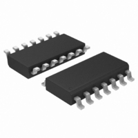
... G −T− SEATING 14 PL PLANE 0.25 (0.010 14X 0.58 *For additional information on our Pb−Free strategy and soldering details, please download the ON Semiconductor Soldering and Mounting Techniques Reference Manual, SOLDERRM/D. PACKAGE DIMENSIONS SOIC−14 CASE 751A−03 ISSUE 0.25 (0.010 ...