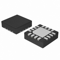
NB7V52MMNG ON Semiconductor, NB7V52MMNG Datasheet - Page 2

NB7V52MMNG
Manufacturer Part Number
NB7V52MMNG
Description
IC FLIP FLOP DIFF RST/CML 16-QFN
Manufacturer
ON Semiconductor
Type
D-Typer
Datasheet
1.NB7V52MMNTXG.pdf
(10 pages)
Specifications of NB7V52MMNG
Function
Reset
Output Type
Differential
Number Of Elements
1
Number Of Bits Per Element
1
Delay Time - Propagation
300ps
Trigger Type
Negative Edge
Operating Temperature
-40°C ~ 85°C
Mounting Type
Surface Mount
Package / Case
16-TQFN Exposed Pad
Lead Free Status / RoHS Status
Lead free / RoHS Compliant
Voltage - Supply
-
Current - Output High, Low
-
Frequency - Clock
-
Available stocks
Company
Part Number
Manufacturer
Quantity
Price
Company:
Part Number:
NB7V52MMNG
Manufacturer:
ON Semiconductor
Quantity:
2
1. In the differential configuration when the input termination pins (VTx, VTx) are connected to a common termination voltage or left open, and
2. All VCC and GND pins must be externally connected to a power supply for proper operation.
Table 1. Pin Description
Pin
10
12
13
14
15
16
11
VTD
VTD
1
2
3
4
5
6
7
8
9
−
if no signal is applied on CLK/CLK input, then the device will be susceptible to self−oscillation.
Figure 2. Pin Configuration (Top View)
D
D
VTCLK
VTCLK
1
2
3
4
Name
VCC
VTD
VTD
CLK
CLK
VEE
VTR
VTR
EP
D
D
Q
Q
R
R
VTCLK
VTR
16
5
CLK CLK VTCLK
NB7V52M
LVPECL, CML,
LVPECL, CML,
LVPECL, CML,
LVPECL, CML,
LVPECL, CML,
LVPECL, CML,
15
6
CML Output
CML Output
R
LVDS Input
LVDS Input
LVDS Input
LVDS Input
LVDS Input
LVDS Input
I/O
14
−
−
−
−
−
−
−
−
−
R
7
VTR
13
8
Internal 50 W Termination Pin for D
Noninverted Differential Data Input. (Note 1)
Inverted Differential Data Input. (Note 1)
Internal 50 W Termination Pin for D
Internal 50 W Termination Pin for CLK
Noninverted Differential Clock Input. (Note 1)
Inverted Differential Clock Input. (Note 1)
Internal 50 W Termination Pin for CLK
Negative Supply Voltage. (Note 2)
Inverted Differential Output
Noninverted Differential Output
Positive Supply Voltage. (Note 2)
Internal 50 W Termination Pin for R
Noninverted Asynchronous Differential Reset Input. (Note 1)
Inverted Asynchronous Differential Reset Input. (Note 1)
Internal 50 W Termination Pin for R
The Exposed Pad (EP) on the QFN−16 package bottom is thermally connected to the die for
improved heat transfer out of package. The exposed pad must be attached to a heat−sinking
conduit. The pad is not electrically connected to the die, but is recommended to be electrically
and thermally connected to VEE on the PC board.
Exposed Pad (EP)
12
10
11
9
VCC
Q
Q
VEE
http://onsemi.com
2
Table 1. INPUT/OUTPUT SELECT TRUTH TABLE
Z = LOW to HIGH Transition
x = Don’t care
R
H
L
L
Description
D
H
L
x
CLK
x
Z
Z
Q
H
L
L


