74ACQ374PC Fairchild Semiconductor, 74ACQ374PC Datasheet
74ACQ374PC
Specifications of 74ACQ374PC


Related parts for 74ACQ374PC


74ACQ374PC Summary of contents
Page 1
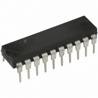
... Device also available in Tape and Reel. Specify by appending suffix letter “X” to the ordering number. Connection Diagram FACT™, Quiet Series™, FACT Quiet Series™, and GTO™ are trademarks of Fairchild Semiconductor Corporation. ©1989 Fairchild Semiconductor Corporation 74ACQ374, 74ACTQ374 Rev. 1.3 ...
Page 2
... IEEE/IEC Logic Diagram Please note that this diagram is provided only for the understanding of logic operations and should not be used to estimate propagation delays. ©1989 Fairchild Semiconductor Corporation 74ACQ374, 74ACTQ374 Rev. 1.3 Functional Description The ACQ/ACTQ374 consists of eight edge-triggered flip- flops with individual D-type inputs and 3-STATE true out- puts ...
Page 3
... O T Operating Temperature A ∆ ∆ t Minimum Input Edge Rate, ACQ Devices: V from 30 ∆V / ∆ t Minimum Input Edge Rate, ACTQ Devices: V from 0.8V to 2.0V ©1989 Fairchild Semiconductor Corporation 74ACQ374, 74ACTQ374 Rev. 1.3 Parameter Parameter , V @ 3.0V, 4.5V, 5. 4.5V, 5. Rating –0.5V to +7.0V –20mA +20mA – ...
Page 4
... Max number of outputs defined as (n). Data inputs are driven 0V to 5V. One output @ GND. 5. Max number of data inputs (n) switching. (n–1) inputs switching (ACQ). Input-under-test switching threshold ( threshold (V ILD ©1989 Fairchild Semiconductor Corporation 74ACQ374, 74ACTQ374 Rev. 1.3 = +25° (V) Conditions Typ ...
Page 5
... Maximum test duration 2.0ms, one output loaded at a time. 8. Max number of outputs defined as (n). Data inputs are driven 0V to 3V. One output @ GND 9. Max number of data inputs (n) switching. (n–1) inputs switching (ACTQ). Input-under-test switching threshold ( threshold (V ILD ©1989 Fairchild Semiconductor Corporation 74ACQ374, 74ACTQ374 Rev. 1.3 = +25° ...
Page 6
... Setup Time, HIGH or LOW Hold Time, HIGH or LOW Pulse Width, HIGH or LOW W Note: 12. Voltage range 5.0 is 5.0V ± 0.5V. Voltage range 3.3 is 3.3V ± 0.3V ©1989 Fairchild Semiconductor Corporation 74ACQ374, 74ACTQ374 Rev. 1.3 = +25° 50pF C L (10) V (V) Min. Typ. Max ...
Page 7
... Hold Time, HIGH or LOW Pulse Width, HIGH or LOW H Note: 15. Voltage range 5.0 is 5.0V ± 0.5V Capacitance Symbol Parameter C Input Capacitance IN C Power Dissipation Capacitance PD ©1989 Fairchild Semiconductor Corporation 74ACQ374, 74ACTQ374 Rev. 1.3 = +25° 50pF C L (13) V (V) Min. Typ. Max. CC 5.0 85 5.0 2.0 7 ...
Page 8
... V are measured with respect to ground OHV OLP reference. 17. Input pulses have the following characteristics 1MHz 3ns 3ns, skew < 150ps Figure 1. Quiet Output Noise Voltage Waveforms ©1989 Fairchild Semiconductor Corporation 74ACQ374, 74ACTQ374 Rev. 1 and OLP OLV OHP OHV ■ Determine the quiet output pin that demonstrates the greatest noise levels ...
Page 9
... Physical Dimensions Dimensions are in inches (millimeters) unless otherwise noted. Figure 3. 20-Lead Small Outline Integrated Circuit (SOIC), JEDEC MS-013, 0.300" Wide ©1989 Fairchild Semiconductor Corporation 74ACQ374, 74ACTQ374 Rev. 1.3 Package Number M20B 9 www.fairchildsemi.com ...
Page 10
... Physical Dimensions (Continued) Dimensions are in millimeters unless otherwise noted. Figure 4. 20-Lead Small Outline Package (SOP), EIAJ TYPE II, 5.3mm Wide ©1989 Fairchild Semiconductor Corporation 74ACQ374, 74ACTQ374 Rev. 1.3 Package Number M20D 10 www.fairchildsemi.com ...
Page 11
... Physical Dimensions (Continued) Dimensions are in millimeters unless otherwise noted. Figure 5. 20-Lead Quarter Size Outline Package (QSOP), JEDEC MO-137, 0.150" Wide ©1989 Fairchild Semiconductor Corporation 74ACQ374, 74ACTQ374 Rev. 1.3 Package Number MQA20 11 www.fairchildsemi.com ...
Page 12
... TRADEMARKS The following are registered and unregistered trademarks Fairchild Semiconductor owns or is authorized to use and is not intended exhaustive list of all such trademarks. ® ACEx Across the board. Around the world. ActiveArray Bottomless Build it Now CoolFET CROSSVOLT CTL™ Current Transfer Logic™ ...