NBSG53ABA ON Semiconductor, NBSG53ABA Datasheet - Page 8
NBSG53ABA
Manufacturer Part Number
NBSG53ABA
Description
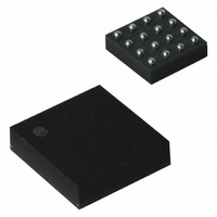
IC FLIP FLOP DIFF CLOCK 16FCBGA
Manufacturer
ON Semiconductor
Type
D-Type Busr
Datasheet
1.NBSG53ABA.pdf
(18 pages)
Specifications of NBSG53ABA
Function
Reset
Output Type
Differential
Number Of Elements
1
Number Of Bits Per Element
2
Frequency - Clock
8GHz
Trigger Type
Positive, Negative
Voltage - Supply
2.375 V ~ 3.465 V
Operating Temperature
-40°C ~ 85°C
Mounting Type
Surface Mount
Package / Case
16-FCBGA
Lead Free Status / RoHS Status
Contains lead / RoHS non-compliant
Current - Output High, Low
-
Delay Time - Propagation
-
Other names
NBSG53ABAOS
Available stocks
Company
Part Number
Manufacturer
Quantity
Price

Company:
Part Number:
NBSG53ABAHTBG
Manufacturer:
ON Semiconductor
Quantity:
10 000
Company:
Part Number:
NBSG53ABAR2
Manufacturer:
ON Semiconductor
Quantity:
10 000


Table 9. DC CHARACTERISTICS, NECL INPUT WITH NECL OUTPUT
V
Symbol
Symbol
NOTE: GigaComm circuits are designed to meet the DC specifications shown in the above table after thermal equilibrium has been estab-
21. Input and output parameters vary 1:1 with V
22. All outputs loaded with 50 W to V
23. V
24. V
25. V
26. V
*Typicals used for testing purposes.
**When an output level of 400 mV is desired and V
***The device packaged in FCBGA-16 have maximum ambient temperature specification of 70 C and devices packaged in QFN-16 have
R
I
I
I
IH
IL
OLS
CC
maximum ambient temperature specification of 85 C.
TIN
input signal.
= 0 V; V
IHCMR
IH
IL
THR
always w V
lished. The circuit is in a test socket or mounted on a printed circuit board and transverse airflow greater than 500 lfpm is maintained.
cannot exceed V
is the voltage applied to one input when running in single-ended mode.
Internal Input Termination Resistor
Input HIGH Current (@V
Input LOW Current (@V
OLS Input Current (See Figure
12)
FLOAT)
(OLS = V
-3.465 V v V
-3.0 V < V
min varies 1:1 with V
EE
= -3.465 V to -2.375 V (Note 21) (continued)
EE
Characteristic
Characteristic
CC
. |V
EE
- 0.8 V, OLS =
CC
IL
(OLS = V
(OLS = V
v -2.375 V
EE
. |V
- V
v -3.0 V
CLK, CLK, D, D
CLK, CLK, D, D
IH
THR
EE
*(OLS = V
(OLS = V
(OLS = V
- V
, V
| < 2600 mV.
CC
CC
IL
IH
CC
THR
IHCMR
)
)
- 0.4 V)
- 1.2 V)
R, SEL
R, SEL
- 2.0 V.
| < 2600 mV.
CC
EE
EE
max varies 1:1 with V
)
)
)
CC
-1500
-1000
-300
Min
.
45
CC
- V
EE
-40 C
http://onsemi.com
-100
-600
-400
Typ
300
100
50
35
20
5
5
5
> 3.0 V, a 2 kW resistor should be connected from OLS to V
NBSG53A
CC
. The V
Max
8
100
100
900
300
100
55
50
50
IHCMR
-1500
-1000
-300
Min
45
range is referenced to the most positive side of the differential
25 C
-100
-600
-400
Typ
300
100
50
35
20
5
5
5
Max
100
100
900
300
100
55
50
50
70 C(BGA)/85 C(QFN)***
-1500
-1000
-300
Min
45
-100
-600
-400
Typ
300
100
50
35
20
5
5
5
EE
.
Max
100
100
900
300
100
55
50
50
Unit
Unit
mA
mA
mA
W
Related parts for NBSG53ABA
Image
Part Number
Description
Manufacturer
Datasheet
Request
R

Part Number:
Description:
ON Semiconductor [VOLTAGE REGULATOR]
Manufacturer:
ON Semiconductor
Datasheet:
Part Number:
Description:
357-036-542-201 CARDEDGE 36POS DL .156 BLK LOPRO
Manufacturer:
ON Semiconductor
Datasheet:
Part Number:
Description:
357-036-542-201 CARDEDGE 36POS DL .156 BLK LOPRO
Manufacturer:
ON Semiconductor
Datasheet:
Part Number:
Description:
357-036-542-201 CARDEDGE 36POS DL .156 BLK LOPRO
Manufacturer:
ON Semiconductor
Datasheet:
Part Number:
Description:
357-036-542-201 CARDEDGE 36POS DL .156 BLK LOPRO
Manufacturer:
ON Semiconductor
Datasheet:
Part Number:
Description:
357-036-542-201 CARDEDGE 36POS DL .156 BLK LOPRO
Manufacturer:
ON Semiconductor
Datasheet:
Part Number:
Description:
357-036-542-201 CARDEDGE 36POS DL .156 BLK LOPRO
Manufacturer:
ON Semiconductor
Datasheet:
Part Number:
Description:
357-036-542-201 CARDEDGE 36POS DL .156 BLK LOPRO
Manufacturer:
ON Semiconductor
Datasheet:
Part Number:
Description:
357-036-542-201 CARDEDGE 36POS DL .156 BLK LOPRO
Manufacturer:
ON Semiconductor
Datasheet:
Part Number:
Description:
357-036-542-201 CARDEDGE 36POS DL .156 BLK LOPRO
Manufacturer:
ON Semiconductor
Datasheet:
Part Number:
Description:
357-036-542-201 CARDEDGE 36POS DL .156 BLK LOPRO
Manufacturer:
ON Semiconductor
Datasheet:
Part Number:
Description:
Manufacturer:
ON Semiconductor
Datasheet:
Part Number:
Description:
Manufacturer:
ON Semiconductor
Datasheet:
Part Number:
Description:
Manufacturer:
ON Semiconductor
Datasheet: