CD40106BCMX Fairchild Semiconductor, CD40106BCMX Datasheet - Page 2
CD40106BCMX
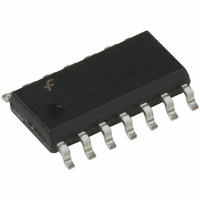
Manufacturer Part Number
CD40106BCMX
Description
IC TRIGGER HEX SCHMITT 14SOIC
Manufacturer
Fairchild Semiconductor
Series
4000Br
Datasheet
1.CD40106BCMX.pdf
(6 pages)
Specifications of CD40106BCMX
Logic Type
Inverter with Schmitt Trigger
Number Of Inputs
1
Number Of Circuits
6
Current - Output High, Low
8.8mA, 8.8mA
Voltage - Supply
3 V ~ 15 V
Operating Temperature
-55°C ~ 125°C
Mounting Type
Surface Mount
Package / Case
14-SOIC (3.9mm Width), 14-SOL
Lead Free Status / RoHS Status
Lead free / RoHS Compliant
Other names
CD40106BCMXTR
Available stocks
Company
Part Number
Manufacturer
Quantity
Price
Company:

Part Number:
CD40106BCMX
Manufacturer:
TI
Quantity:
12 000
Part Number:
CD40106BCMX
Manufacturer:
ON/ه®‰و£®ç¾ژ
Quantity:
20 000


www.fairchildsemi.com
I
V
V
V
V
V
I
I
I
DD
OL
OH
IN
Absolute Maximum Ratings
(Note 2)
DC Electrical Characteristics
Note 3: I
Symbol
OL
OH
T
T
H
DC Supply Voltage (V
Input Voltage (V
Storage Temperature Range (T
Power Dissipation (P
Lead Temperature (T
Dual-In-Line
Small Outline
(Soldering, 10 seconds)
OH
Quiescent Device Current
LOW Level Output
Voltage
HIGH Level Output
Voltage
Negative-Going Threshold
Voltage
Positive-Going Threshold
Voltage
Hysteresis (V
Voltage
LOW Level Output
Current (Note 3)
HIGH Level Output
Current (Note 3)
Input Current
and I
OL
are tested one output at a time.
IN
)
Parameter
T
D
L
DD
)
)
V
)
T
)
S
)
V
V
V
|I
V
V
V
|I
V
V
V
V
V
V
V
V
V
V
V
V
V
V
V
V
V
V
V
V
0.5 to V
O
O
DD
DD
DD
DD
DD
DD
DD
DD
DD
DD
DD
DD
DD
DD
DD
DD
DD
DD
DD
DD
DD
DD
DD
DD
DD
DD
|
|
1 A
1 A
65 C to 150 C
5V
10V
15V
5V
10V
15V
5V
10V
15V
5V, V
10V, V
15V, V
5V, V
10V, V
15V, V
5V
10V
15V
5V, V
10V, V
15V, V
5V, V
10V, V
15V, V
15V, V
15V, V
0.5 to 18 V
(Note 1)
DD
Conditions
O
O
O
O
(Note 3)
O
O
O
O
O
O
O
O
IN
IN
700 mW
500 mW
0.5 V
4.5V
0.5V
0.4V
4.6V
9V
13.5V
1V
1.5V
0.5V
1.5V
9.5V
13.5V
260 C
0V
15V
DC
DC
2
Recommended Operating
Note 1: “Absolute Maximum Ratings” are those values beyond which the
safety of the device cannot be guaranteed. They are not meant to imply
that the devices should be operated at these limits. The table of “Recom-
mended Operating Conditions” and “Electrical Characteristics” provides
conditions for actual device operation.
Note 2: V
Conditions
DC Supply Voltage (V
Input Voltage (V
Operating Temperature Range (T
14.95
4.95
9.95
0.64
Min
0.7
1.4
2.1
3.0
6.0
9.0
1.0
2.0
3.0
1.6
4.2
0.64
1.6
4.2
SS
55 C
0V unless otherwise specified.
Max
0.05
0.05
0.05
12.9
10.8
1.0
2.0
4.0
2.0
4.0
6.0
4.3
8.6
3.6
7.2
0.1
0.1
IN
)
14.95
4.95
9.95
0.51
Min
0.7
1.4
2.1
3.0
6.0
9.0
1.0
2.0
3.0
1.3
3.4
0.51
(Note 2)
1.3
3.4
DD
)
10
10.0
0.88
2.25
25 C
Typ
10
1.4
3.2
5.0
3.6
6.8
2.2
3.6
5.0
8.8
0.88
2.25
10
15
8.8
5
5
5
Max
0.05
0.05
0.05
12.9
10.8
A
1.0
2.0
4.0
2.0
4.0
6.0
4.3
8.6
3.6
7.2
0.1
0.1
)
14.95
4.95
0.95
0.36
Min
0.7
1.4
2.1
3.0
6.0
9.0
1.0
2.0
3.0
0.9
2.4
0.36
0.9
2.4
55 C to 125 C
125 C
0 to V
3 to 15 V
Max
0.05
0.05
0.05
12.9
10.8
120
2.0
4.0
6.0
4.3
8.6
3.6
7.2
1.0
30
60
1.0
DD
V
Units
mA
mA
DC
DC
V
V
V
V
V
A
A
Related parts for CD40106BCMX
Image
Part Number
Description
Manufacturer
Datasheet
Request
R

Part Number:
Description:
Manufacturer:
Fairchild Semiconductor
Datasheet:
Part Number:
Description:
IC BUFFER HEX NON-INV 16DIP
Manufacturer:
Fairchild Semiconductor
Datasheet:

Part Number:
Description:
Monostable Multivibrator Monostable Multivib
Manufacturer:
Fairchild Semiconductor
Datasheet:
Part Number:
Description:
Fairchild Semiconductor [IGBT MODULE]
Manufacturer:
Fairchild Semiconductor
Datasheet:

Part Number:
Description:
Discrete Semiconductor Modules
Manufacturer:
Fairchild Semiconductor
Part Number:
Description:
Discrete Semiconductor Modules
Manufacturer:
Fairchild Semiconductor
Part Number:
Description:
This N-Channel MOSFET is produced using Fairchild Semiconductor’s advanced Power Trench® process
Manufacturer:
Fairchild Semiconductor
Datasheet:
Part Number:
Description:
This N-Channel MOSFET is produced using Fairchild Semiconductor’s advanced Power Trench® process
Manufacturer:
Fairchild Semiconductor
Datasheet:
Part Number:
Description:
This N-Channel MOSFET is produced using Fairchild Semiconductor’s advanced PowerTrench® process
Manufacturer:
Fairchild Semiconductor
Datasheet:
Part Number:
Description:
This N-Channel MOSFET is produced using Fairchild Semiconductor’s advanced PowerTrench® process
Manufacturer:
Fairchild Semiconductor
Datasheet:
Part Number:
Description:
This N-Channel MOSFET is produced using Fairchild Semiconductor’s advanced Power Trench® process
Manufacturer:
Fairchild Semiconductor
Datasheet:
Part Number:
Description:
This N-Channel logic Level MOSFETs are produced using Fairchild Semiconductor‘s advanced Power Trench® process that has been special tailored to minimize the on-state resistance and yet maintain superior switching performance
Manufacturer:
Fairchild Semiconductor
Datasheet:
Part Number:
Description:
This N-Channel MOSFET is produced using Fairchild Semiconductor’s advanced Power Trench® process
Manufacturer:
Fairchild Semiconductor
Datasheet: