CD4011BCM Fairchild Semiconductor, CD4011BCM Datasheet
CD4011BCM
Specifications of CD4011BCM
Available stocks


Related parts for CD4011BCM


CD4011BCM Summary of contents
Page 1
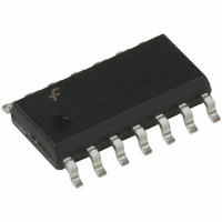
... M14D 14-Lead Small Outline Package (SOP), EIAJ TYPE II, 5.3mm Wide CD4001BCN N14A 14-Lead Plastic Dual-In-Line Package (PDIP), JEDEC MS-001, 0.300” Wide CD4011BCM M14A 14-Lead Small Outline Integrated Circuit (SOIC), JEDEC MS-120, 0.150” Narrow CD4011BCN N14A 14-Lead Plastic Dual-In-Line Package (PDIP), JEDEC MS-001, 0.300” Wide Devices also available in Tape and Reel. Specify by appending the suffix letter “ ...
Page 2
Schematic Diagrams www.fairchildsemi.com CD4001BC device shown Logical “1” HIGH Logical “0” LOW All inputs protected by standard CMOS protection circuit. CD4011BC device shown • B Logical “1” ...
Page 3
Absolute Maximum Ratings (Note 2) Voltage at any Pin 0. Power Dissipation ( Dual-In-Line Small Outline V Range 0 Storage Temperature ( Lead Temperature ( (Soldering, 10 seconds) DC Electrical ...
Page 4
AC Electrical Characteristics CD4011BC Input ns pF Symbol Parameter t Propagation Delay, PHL HIGH-to-LOW Level t Propagation Delay, PLH LOW-to-HIGH Level Transition Time ...
Page 5
Typical Transfer Characteristics 5 www.fairchildsemi.com ...
Page 6
www.fairchildsemi.com 6 ...
Page 7
Physical Dimensions inches (millimeters) unless otherwise noted 14-Lead Small Outline Integrated Circuit (SOIC), JEDEC MS-120, 0.150” Narrow 14-Lead Small Outline Package (SOP), EIAJ TYPE II, 5.3mm Wide Package Number M14A Package Number M14D 7 www.fairchildsemi.com ...
Page 8
Physical Dimensions inches (millimeters) unless otherwise noted (Continued) 14-Lead Plastic Dual-In-Line Package (PDIP), JEDEC MS-001, 0.300” Wide LIFE SUPPORT POLICY FAIRCHILD’S PRODUCTS ARE NOT AUTHORIZED FOR USE AS CRITICAL COMPONENTS IN LIFE SUPPORT DEVICES OR SYSTEMS WITHOUT THE EXPRESS WRITTEN ...