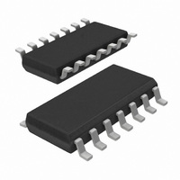
74LV14D,118 NXP Semiconductors, 74LV14D,118 Datasheet - Page 6

74LV14D,118
Manufacturer Part Number
74LV14D,118
Description
IC HEX INV SCHMITT TRIG 14SOIC
Manufacturer
NXP Semiconductors
Series
74LVr
Datasheet
1.74LV14D118.pdf
(19 pages)
Specifications of 74LV14D,118
Number Of Circuits
6
Logic Type
Inverter with Schmitt Trigger
Package / Case
14-SOIC (3.9mm Width), 14-SOL
Number Of Inputs
1
Current - Output High, Low
12mA, 12mA
Voltage - Supply
1 V ~ 5.5 V
Operating Temperature
-40°C ~ 125°C
Mounting Type
Surface Mount
Logic Family
LV
High Level Output Current
- 12 mA
Low Level Output Current
12 mA
Supply Voltage (max)
5.5 V
Supply Voltage (min)
1 V
Maximum Operating Temperature
+ 125 C
Mounting Style
SMD/SMT
Operating Supply Voltage
3.3 V
Logical Function
Inverter Schmit Trig
Number Of Elements
6
Input Type
Schmitt Trigger
Propagation Delay Time
48ns
Operating Supply Voltage (typ)
3.3V
Package Type
SO
Operating Temp Range
-40C to 125C
Pin Count
14
Quiescent Current
40uA
Output Type
Schmitt Trigger
Technology
CMOS
Mounting
Surface Mount
Operating Temperature Classification
Automotive
Operating Supply Voltage (max)
5.5V
Operating Supply Voltage (min)
1V
Lead Free Status / RoHS Status
Lead free / RoHS Compliant
Lead Free Status / RoHS Status
Lead free / RoHS Compliant, Lead free / RoHS Compliant
Other names
74LV14D-T
74LV14D-T
935069490118
74LV14D-T
935069490118
NXP Semiconductors
11. Dynamic characteristics
Table 7.
GND = 0 V; For test circuit see
[1]
[2]
[3]
[4]
12. Waveforms
74LV14
Product data sheet
Symbol Parameter
t
C
pd
Fig 6. The input (nA) to output (nY) propagation delays
PD
All typical values are measured at T
t
Typical values are measured at nominal supply voltage (V
C
P
f
C
V
N = number of inputs switching
(C
pd
i
D
CC
PD
= input frequency in MHz, f
L
is the same as t
= output load capacitance in pF
= C
L
is used to determine the dynamic power dissipation (P
= supply voltage in V
V
Measurement points are given in
propagation delay
power dissipation
capacitance
V
PD
OL
Dynamic characteristics
CC
V
2
and V
f
CC
o
2
) = sum of the outputs.
OH
f
PLH
i
are typical voltage output levels that occur with the output load.
N + (C
and t
PHL
o
Conditions
nA to nY; see
V
V
V
V
V
V
C
V
Figure
= output frequency in MHz
L
CC
CC
CC
CC
CC
CC
I
L
.
V
= GND to V
= 50 pF; f
= 1.2 V
= 2.0 V
= 2.7 V
= 3.0 V to 3.6 V; C
= 3.0 V to 3.6 V
= 4.5 V to 5.5 V
CC
amb
nY output
nA input
7.
2
Table
f
= 25 C.
o
All information provided in this document is subject to legal disclaimers.
) where:
i
= 1 MHz;
Figure 6
8.
CC
GND
V
V
OH
OL
V
I
Rev. 5 — 5 January 2011
L
= 15 pF
CC
D
V
in W).
= 3.3 V).
M
V
M
t
PHL
[2]
[3]
[3]
[4]
Min
-
-
-
-
-
-
-
T
amb
to +85 C
V
Typ
M
= 40 C
80
27
20
13
15
15
V
-
mna344
M
[1]
t
PLH
Max
37
28
22
18
-
-
-
Hex inverting Schmitt trigger
Min
T
-
-
-
-
-
-
-
amb
to +125 C
= 40 C
© NXP B.V. 2011. All rights reserved.
74LV14
Max
48
35
28
23
-
-
-
6 of 19
Unit
ns
ns
ns
ns
ns
ns
pF


