HCF4001BEY STMicroelectronics, HCF4001BEY Datasheet - Page 2
HCF4001BEY
Manufacturer Part Number
HCF4001BEY
Description
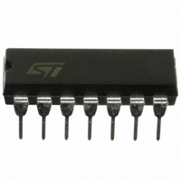
IC GATE NOR QUAD 2INP 14-DIP
Manufacturer
STMicroelectronics
Series
4000Br
Specifications of HCF4001BEY
Logic Type
NOR Gate
Number Of Inputs
2
Number Of Circuits
4
Current - Output High, Low
6.8mA, 6.8mA
Voltage - Supply
3 V ~ 20 V
Operating Temperature
-55°C ~ 125°C
Mounting Type
Through Hole
Package / Case
14-DIP (0.300", 7.62mm)
Logic Family
4000B
Logical Function
NOR
Number Of Elements
4
High Level Output Current
-2.4mA
Low Level Output Current
2.4mA
Propagation Delay Time
80ns
Operating Supply Voltage (typ)
3.3/5/9/12/15/18V
Operating Temp Range
-55C to 125C
Package Type
PDIP
Number Of Outputs
1
Technology
CMOS
Mounting
Through Hole
Pin Count
14
Operating Temperature Classification
Military
Quiescent Current
5uA
Operating Supply Voltage (max)
20V
Operating Supply Voltage (min)
3V
Product
NOR
Supply Voltage (max)
20 V
Supply Voltage (min)
3 V
Maximum Operating Temperature
+ 125 C
Mounting Style
Through Hole
Minimum Operating Temperature
- 55 C
Circuit Type
Monolithic Integrated
Current, Supply
150 μA
Function Type
2-Inputs
Logic Function
NOR Gate
Temperature, Operating, Range
-55 to +125 °C
Voltage, Supply
3 to 20 V
Output Current
6.8mA
No. Of Inputs
2
Supply Voltage Range
3V To 20V
Logic Case Style
DIP
No. Of Pins
14
Operating Temperature Range
-55°C To +125°C
Ic Generic Number
4001
Rohs Compliant
Yes
Lead Free Status / RoHS Status
Lead free / RoHS Compliant
Other names
497-1340-5
Available stocks
Company
Part Number
Manufacturer
Quantity
Price
Company:

Part Number:
HCF4001BEY
Manufacturer:
ST
Quantity:
15 000


HCF4001B
INPUT EQUIVALENT CIRCUIT
LOGIC DIAGRAM
ABSOLUTE MAXIMUM RATINGS
Absolute Maximum Ratings are those values beyond which damage to the device may occur. Functional operation under these conditions is
not implied.
All voltage values are referred to V
RECOMMENDED OPERATING CONDITIONS
2/8
Symbol
Symbol
V
V
T
T
T
P
V
V
stg
DD
I
DD
op
op
I
D
I
I
Supply Voltage
DC Input Voltage
DC Input Current
Power Dissipation per Package
Power Dissipation per Output Transistor
Operating Temperature
Storage Temperature
Supply Voltage
Input Voltage
Operating Temperature
SS
pin voltage.
Parameter
Parameter
PIN DESCRIPTION
TRUTH TABLE
1, 2, 5, 6, 8,
3, 4, 10, 11
9, 12, 13
PIN N°
A, C, E, G
14
7
H
H
L
L
INPUTS
A, B, C, D, E,
SYMBOL
J, K, L, M
F, G, H
V
V
DD
SS
B, D, F, H
-0.5 to V
-55 to +125
-65 to +150
-0.5 to +22
-55 to 125
H
H
L
L
0 to V
3 to 20
Value
Value
Data Inputs
Data Outputs
Negative Supply Voltage
Positive Supply Voltage
200
100
NAME AND FUNCTION
10
DD
DD
+ 0.5
OUTPUTS
J, K, L, M
H
L
L
L
Unit
Unit
mW
mW
mA
°C
°C
°C
V
V
V
V
Related parts for HCF4001BEY
Image
Part Number
Description
Manufacturer
Datasheet
Request
R

Part Number:
Description:
NOR GATE
Manufacturer:
STMICROELECTRONICS [STMicroelectronics]
Datasheet:

Part Number:
Description:
STMicroelectronics [RIPPLE-CARRY BINARY COUNTER/DIVIDERS]
Manufacturer:
STMicroelectronics
Datasheet:
Part Number:
Description:
STMicroelectronics [LIQUID-CRYSTAL DISPLAY DRIVERS]
Manufacturer:
STMicroelectronics
Datasheet:

Part Number:
Description:
BOARD EVAL FOR MEMS SENSORS
Manufacturer:
STMicroelectronics
Datasheet:
Part Number:
Description:
NPN TRANSISTOR POWER MODULE
Manufacturer:
STMicroelectronics
Datasheet:
Part Number:
Description:
TURBOSWITCH ULTRA-FAST HIGH VOLTAGE DIODE
Manufacturer:
STMicroelectronics
Datasheet:
Part Number:
Description:
Manufacturer:
STMicroelectronics
Datasheet:
Part Number:
Description:
DIODE / SCR MODULE
Manufacturer:
STMicroelectronics
Datasheet:
Part Number:
Description:
DIODE / SCR MODULE
Manufacturer:
STMicroelectronics
Datasheet:
Part Number:
Description:
Search -----> STE16N100
Manufacturer:
STMicroelectronics
Datasheet:
Part Number:
Description:
Search ---> STE53NA50
Manufacturer:
STMicroelectronics
Datasheet:
Part Number:
Description:
NPN Transistor Power Module
Manufacturer:
STMicroelectronics
Datasheet: