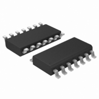
MC14082BDG ON Semiconductor, MC14082BDG Datasheet - Page 7

MC14082BDG
Manufacturer Part Number
MC14082BDG
Description
IC GATE AND DUAL CMOS 14SOIC
Manufacturer
ON Semiconductor
Series
4000Br
Datasheet
1.MC14011BDR2G.pdf
(14 pages)
Specifications of MC14082BDG
Logic Type
AND Gate
Number Of Inputs
4
Number Of Circuits
2
Current - Output High, Low
3.4mA, 3.4mA
Voltage - Supply
3 V ~ 18 V
Operating Temperature
-55°C ~ 125°C
Mounting Type
Surface Mount
Package / Case
14-SOIC (3.9mm Width), 14-SOL
Output Current
8.8mA
No. Of Inputs
4
Supply Voltage Range
3V To 18V
Logic Case Style
SOIC
No. Of Pins
14
Operating Temperature Range
-55°C To +125°C
Termination Type
SMD
Rohs Compliant
Yes
Logic Family
4000
Logical Function
AND
Number Of Elements
2
High Level Output Current
-4.2mA
Low Level Output Current
4.2mA
Operating Supply Voltage (typ)
3.3/5/9/12/15V
Operating Temp Range
-55C to 125C
Package Type
SOIC
Number Of Outputs
1
Technology
CMOS
Mounting
Surface Mount
Pin Count
14
Operating Temperature Classification
Military
Quiescent Current
1uA
Operating Supply Voltage (max)
18V
Operating Supply Voltage (min)
3V
Filter Terminals
SMD
Family Type
CD4000B
Lead Free Status / RoHS Status
Lead free / RoHS Compliant
Other names
MC14082BDGOS
Available stocks
Company
Part Number
Manufacturer
Quantity
Price
Part Number:
MC14082BDG
Manufacturer:
ON/安森美
Quantity:
20 000
5.0
4.0
3.0
2.0
1.0
8.0
6.0
4.0
2.0
16
14
12
10
0
0
0
0
1.0
2.0
Figure 10. V
2.0
4.0
Figure 8. V
V
V
V
V
O
O
out
V
in
in
, INPUT VOLTAGE (Vdc)
3.0
, INPUT VOLTAGE (Vdc)
6.0
0
SINGLE INPUT NAND, AND
MULTIPLE INPUT NOR, OR
(a) Inverting Function
V
TYPICAL B−SERIES GATE CHARACTERISTICS (cont’d)
SINGLE INPUT NOR, OR
MULTIPLE INPUT NAND, AND
DD
DD
4.0
DD
8.0
= 15 Vdc
V
= 5.0 Vdc
IL
SINGLE INPUT NOR, OR
MULTIPLE INPUT NAND, AND
SINGLE INPUT NAND, AND
MULTIPLE INPUT NOR, OR
5.0
10
VOLTAGE TRANSFER CHARACTERISTICS
V
Figure 11. DC Noise Immunity
IH
http://onsemi.com
V
V
DD
in
V
SS
= 0 VOLTS DC
7
from an ideal “1” or “0” input level which does not produce
output state change(s). The typical and guaranteed limit
values of the input values V
be at a fixed voltage V
Characteristics table. V
in Figure 11.
“0” levels =
The DC noise margin is defined as the input voltage range
Guaranteed minimum noise margins for both the “1” and
V
V
V
O
O
out
8.0
6.0
4.0
2.0
10
0
(b) Non−Inverting Function
0
0
1.0 V with a 5.0 V supply
2.0 V with a 10.0 V supply
2.5 V with a 15.0 V supply
V
DD
2.0
V
IL
4.0
DC NOISE MARGIN
Figure 9. V
V
IL
in
, INPUT VOLTAGE (Vdc)
6.0
and V
V
O
IH
SINGLE INPUT NAND, AND
MULTIPLE INPUT NOR, OR
IL
are given in the Electrical
SINGLE INPUT NOR, OR
MULTIPLE INPUT NAND, AND
and V
IH
8.0
DD
V
V
are presented graphically
DD
in
= 10 Vdc
IH
10
for the output(s) to


