MC14025BCPG ON Semiconductor, MC14025BCPG Datasheet - Page 6
MC14025BCPG
Manufacturer Part Number
MC14025BCPG
Description
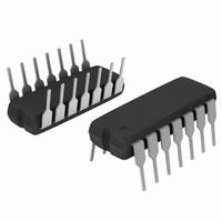
IC GATE NOR TRIPLE CMOS 14DIP
Manufacturer
ON Semiconductor
Series
4000Br
Specifications of MC14025BCPG
Logic Type
NOR Gate
Number Of Inputs
3
Number Of Circuits
3
Current - Output High, Low
3.4mA, 3.4mA
Voltage - Supply
3 V ~ 18 V
Operating Temperature
-55°C ~ 125°C
Mounting Type
Through Hole
Package / Case
14-DIP (0.300", 7.62mm)
Circuit Type
Low-Power Schottky
Current, Supply
30 μA
Function Type
3-Inputs
Logic Function
NOR Gate
Package Type
PDIP-14
Temperature, Operating, Range
-55 to +125 °C
Voltage, Supply
3 to 18 VDC
Output Current
8.8mA
No. Of Inputs
3
Supply Voltage Range
3V To 18V
Logic Case Style
DIP
No. Of Pins
14
Operating Temperature Range
-55°C To +125°C
Filter Terminals
DIP
Rohs Compliant
Yes
Family Type
4000 CMOS
Lead Free Status / RoHS Status
Lead free / RoHS Compliant
Other names
MC14025BCPGOS
Available stocks
Company
Part Number
Manufacturer
Quantity
Price

Part Number:
MC14025BCPG
Manufacturer:
ON/安森美
Quantity:
20 000


5.0
4.0
3.0
2.0
1.0
8.0
6.0
4.0
2.0
5.0
20
18
16
14
12
10
50
45
40
35
30
25
20
15
10
0
0
0
0
0
0
1.0
2.0
N−CHANNEL DRAIN CURRENT (SINK)
1.0
2.0
4.0
V
V
V
DS
DS
DS
, DRAIN-TO-SOURCE VOLTAGE (Vdc)
, DRAIN-TO-SOURCE VOLTAGE (Vdc)
, DRAIN-TO-SOURCE VOLTAGE (Vdc)
Figure 2. V
Figure 4. V
Figure 6. V
3.0
6.0
2.0
4.0
8.0
5.0
GS
10
GS
GS
Caution: The maximum rating for output current is 10 mA per pin.
= 5.0 Vdc
= 10 Vdc
= 15 Vdc
T
TYPICAL B−SERIES GATE CHARACTERISTICS
3.0
A
These typical curves are not guarantees, but are design aids.
6.0
12
= - 55°C
+ 25°C
+ 125°C
- 40°C
7.0
14
+ 85°C
T
A
+ 85°C
- 40°C
+ 25°C
+ 85°C
+ 125°C
= - 55°C
T
4.0
8.0
16
A
= - 55°C
- 40°C
+ 125°C
+ 25°C
9.0
18
http://onsemi.com
5.0
10
20
6
- 100
- 9.0
- 8.0
- 7.0
- 6.0
- 5.0
- 4.0
- 3.0
- 2.0
- 1.0
- 5.0
- 10
- 50
- 45
- 40
- 35
- 30
- 25
- 20
- 15
- 10
- 90
- 80
- 70
- 60
- 50
- 40
- 30
- 20
- 10
0
0
0
0
0
0
- 1.0
- 2.0
P−CHANNEL DRAIN CURRENT (SOURCE)
- 1.0
- 2.0
- 4.0
V
V
V
DS
DS
DS
Figure 3. V
, DRAIN-TO-SOURCE VOLTAGE (Vdc)
, DRAIN-TO-SOURCE VOLTAGE (Vdc)
, DRAIN-TO-SOURCE VOLTAGE (Vdc)
Figure 5. V
Figure 7. V
- 3.0
- 6.0
- 8.0
- 2.0
- 4.0
- 5.0
GS
- 10
GS
GS
= − 5.0 Vdc
= − 10 Vdc
= − 15 Vdc
T
- 3.0
- 6.0
- 12
A
= - 55°C
+ 25°C
- 7.0
+ 125°C
- 14
T
+ 85°C
A
+ 25°C
T
= - 55°C
A
- 4.0
- 8.0
= - 55°C
- 16
- 40°C
- 40°C
+ 85°C
+ 125°C
+ 125°C
+ 85°C
+ 25°C
- 9.0
- 40°C
- 18
- 5.0
- 10
- 20
Related parts for MC14025BCPG
Image
Part Number
Description
Manufacturer
Datasheet
Request
R

Part Number:
Description:
CONTACTOR, 1NO, 110VAC, 14A, DIN RAIL
Manufacturer:
IMO PRECISION CONTROLS
Datasheet:
Part Number:
Description:
CONTACTOR, 1NO, 230VAC, 14A, DIN RAIL
Manufacturer:
IMO PRECISION CONTROLS
Datasheet:
Part Number:
Description:
CONTACTOR, 1NO, 24VAC, 14A, DIN RAIL
Manufacturer:
IMO PRECISION CONTROLS
Datasheet:

Part Number:
Description:
ON Semiconductor [VOLTAGE REGULATOR]
Manufacturer:
ON Semiconductor
Datasheet:
Part Number:
Description:
357-036-542-201 CARDEDGE 36POS DL .156 BLK LOPRO
Manufacturer:
ON Semiconductor
Datasheet:
Part Number:
Description:
357-036-542-201 CARDEDGE 36POS DL .156 BLK LOPRO
Manufacturer:
ON Semiconductor
Datasheet:
Part Number:
Description:
357-036-542-201 CARDEDGE 36POS DL .156 BLK LOPRO
Manufacturer:
ON Semiconductor
Datasheet:
Part Number:
Description:
357-036-542-201 CARDEDGE 36POS DL .156 BLK LOPRO
Manufacturer:
ON Semiconductor
Datasheet:
Part Number:
Description:
357-036-542-201 CARDEDGE 36POS DL .156 BLK LOPRO
Manufacturer:
ON Semiconductor
Datasheet:
Part Number:
Description:
357-036-542-201 CARDEDGE 36POS DL .156 BLK LOPRO
Manufacturer:
ON Semiconductor
Datasheet:
Part Number:
Description:
357-036-542-201 CARDEDGE 36POS DL .156 BLK LOPRO
Manufacturer:
ON Semiconductor
Datasheet:
Part Number:
Description:
357-036-542-201 CARDEDGE 36POS DL .156 BLK LOPRO
Manufacturer:
ON Semiconductor
Datasheet:
Part Number:
Description:
357-036-542-201 CARDEDGE 36POS DL .156 BLK LOPRO
Manufacturer:
ON Semiconductor
Datasheet:
Part Number:
Description:
357-036-542-201 CARDEDGE 36POS DL .156 BLK LOPRO
Manufacturer:
ON Semiconductor
Datasheet: