74HCT132N,652 NXP Semiconductors, 74HCT132N,652 Datasheet - Page 2
74HCT132N,652
Manufacturer Part Number
74HCT132N,652
Description
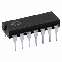
IC TRIGGER NAND QUAD 2IN 14DIP
Manufacturer
NXP Semiconductors
Series
74HCTr
Datasheets
1.74HCT4046ADB112.pdf
(19 pages)
2.74HCT4046ADB112.pdf
(23 pages)
3.74HC132N652.pdf
(8 pages)
Specifications of 74HCT132N,652
Number Of Circuits
4
Package / Case
14-DIP (0.300", 7.62mm)
Logic Type
NAND Gate - Schmitt Trigger
Number Of Inputs
2
Current - Output High, Low
5.2mA, 5.2mA
Voltage - Supply
4.5 V ~ 5.5 V
Operating Temperature
-40°C ~ 125°C
Mounting Type
Through Hole
Product
NAND
Logic Family
74HCT
High Level Output Current
- 4 mA
Low Level Output Current
4 mA
Propagation Delay Time
17 ns
Supply Voltage (max)
5.5 V
Supply Voltage (min)
4.5 V
Maximum Operating Temperature
+ 125 C
Mounting Style
SMD/SMT
Minimum Operating Temperature
- 40 C
Logical Function
NAND
Number Of Elements
4
Operating Supply Voltage (typ)
5V
Operating Temp Range
-40C to 125C
Package Type
PDIP
Number Of Outputs
1
Technology
CMOS
Mounting
Through Hole
Pin Count
14
Operating Temperature Classification
Automotive
Quiescent Current
2uA
Operating Supply Voltage (max)
5.5V
Operating Supply Voltage (min)
4.5V
Lead Free Status / RoHS Status
Lead free / RoHS Compliant
Lead Free Status / RoHS Status
Lead free / RoHS Compliant, Lead free / RoHS Compliant
Other names
568-1511-5
74HCT132N
933669150652
74HCT132N
933669150652


Philips Semiconductors
FEATURES
GENERAL DESCRIPTION
The 74HC/HCT132 are high-speed Si-gate CMOS devices and are pin compatible with low power Schottky TTL (LSTTL).
They are specified in compliance with JEDEC standard no. 7A.
The 74HC/HCT132 contain four 2-input NAND gates which accept standard input signals. They are capable of
transforming slowly changing input signals into sharply defined, jitter-free output signals.
The gate switches at different points for positive and negative-going signals. The difference between the positive voltage
V
QUICK REFERENCE DATA
GND = 0 V; T
Notes
1. C
2. For HC the condition is V
ORDERING INFORMATION
See
September 1993
SYMBOL
t
C
C
T
PHL
Output capability: standard
I
Quad 2-input NAND Schmitt trigger
I
PD
CC
f
f
C
V
For HCT the condition is V
and the negative voltage V
i
o
“74HC/HCT/HCU/HCMOS Logic Package Information”
/ t
CC
PD
= input frequency in MHz
L
category: SSI
= output frequency in MHz
PLH
(C
= output load capacitance in pF
P
= supply voltage in V
is used to determine the dynamic power dissipation (P
D
L
= C
V
amb
CC
PD
2
= 25 C; t
PARAMETER
propagation delay nA, nB to nY
input capacitance
power dissipation capacitance per gate
V
f
o
CC
) = sum of outputs
2
f
r
i
= t
I
= GND to V
I
f
T
= GND to V
= 6 ns
(C
is defined as the hysteresis voltage V
L
V
CC
2
CC
CC
f
o
) where:
1.5 V
2
.
CONDITIONS
C
notes 1 and 2
L
D
= 15 pF; V
in W):
H
.
CC
= 5 V 11
3.5
24
HC
TYPICAL
74HC/HCT132
Product specification
17
3.5
20
HCT
ns
pF
pF
UNIT
Related parts for 74HCT132N,652
Image
Part Number
Description
Manufacturer
Datasheet
Request
R

Part Number:
Description:
IC BUFF/DVR TRI-ST DUAL 20DIP
Manufacturer:
Fairchild Semiconductor
Datasheet:

Part Number:
Description:
IC BUS TRANSCVR 3-ST 8BIT 20DIP
Manufacturer:
ON Semiconductor
Datasheet:

Part Number:
Description:
IC TRANSCEIVER 3-ST 8BIT 20SOIC
Manufacturer:
Fairchild Semiconductor
Datasheet:

Part Number:
Description:
IC BUFFER NONINV QUAD 3ST 14SOIC
Manufacturer:
ON Semiconductor
Datasheet:
Part Number:
Description:
IC BUFFER NONINV QUAD 3ST 14SOIC
Manufacturer:
ON Semiconductor
Datasheet:

Part Number:
Description:
IC BUS TRANSCVR 3-ST 8BIT 20SOIC
Manufacturer:
ON Semiconductor
Datasheet:

Part Number:
Description:
IC BUFF/DVR TRI-ST 8BIT 20SOIC
Manufacturer:
ON Semiconductor
Datasheet:

Part Number:
Description:
IC FLIP FLOP OCT D 3ST 20TSSOP
Manufacturer:
Fairchild Semiconductor
Datasheet:

Part Number:
Description:
IC FLIP FLOP OCTAL D 20-DIP
Manufacturer:
STMicroelectronics
Datasheet:

Part Number:
Description:
IC FLIP FLOP DUAL D-TYPE 14-SOIC
Manufacturer:
Fairchild Semiconductor
Datasheet:
Part Number:
Description:
IC FLIP FLOP OCTAL D 20-SOIC
Manufacturer:
Fairchild Semiconductor
Datasheet:

Part Number:
Description:
IC FLIP FLOP OCT D 3ST 20-SOIC
Manufacturer:
ON Semiconductor
Datasheet:

Part Number:
Description:
IC INVERT HEX SCHM TRIG 14-SOIC
Manufacturer:
ON Semiconductor
Datasheet:

Part Number:
Description:
IC INVERTER HEX LSTTL IN 14TSSOP
Manufacturer:
ON Semiconductor
Datasheet:
Part Number:
Description:
IC INVERT HEX SCHM TRIG 14TSSOP
Manufacturer:
ON Semiconductor
Datasheet: