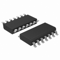
MC74AC00DR2G ON Semiconductor, MC74AC00DR2G Datasheet - Page 3

MC74AC00DR2G
Manufacturer Part Number
MC74AC00DR2G
Description
IC GATE NAND QUAD 2INPUT 14SOIC
Manufacturer
ON Semiconductor
Series
74ACr
Datasheet
1.MC74AC00DG.pdf
(10 pages)
Specifications of MC74AC00DR2G
Logic Type
NAND Gate
Number Of Inputs
2
Number Of Circuits
4
Current - Output High, Low
24mA, 24mA
Voltage - Supply
2 V ~ 6 V
Operating Temperature
-55°C ~ 125°C
Mounting Type
Surface Mount
Package / Case
14-SOIC (3.9mm Width), 14-SOL
Product
NAND
Logic Family
74AC
High Level Output Current
- 24 mA
Low Level Output Current
24 mA
Propagation Delay Time
9.5 ns
Supply Voltage (max)
6 V
Supply Voltage (min)
2 V
Maximum Operating Temperature
+ 125 C
Mounting Style
SMD/SMT
Minimum Operating Temperature
- 55 C
Output Current
24mA
No. Of Inputs
2
Supply Voltage Range
2V To 6V
Logic Case Style
SOIC
No. Of Pins
14
Operating Temperature Range
-55°C To +125°C
Filter Terminals
SMD
Rohs Compliant
Yes
Family Type
AC
Lead Free Status / RoHS Status
Lead free / RoHS Compliant
Other names
MC74AC00DR2GOS
MC74AC00DR2GOS
MC74AC00DR2GOSTR
MC74AC00DR2GOS
MC74AC00DR2GOSTR
Available stocks
Company
Part Number
Manufacturer
Quantity
Price
Part Number:
MC74AC00DR2G
Manufacturer:
ON/安森美
Quantity:
20 000
DC CHARACTERISTICS
*All outputs loaded; thresholds on input associated with output under test.
†Maximum test duration 2.0 ms, one output loaded at a time.
NOTE:
AC CHARACTERISTICS
*Voltage Range 3.3 V is 3.3 V $0.3 V.
Symbol
Symbol
V
V
V
V
I
I
I
I
t
t
IN
OLD
OHD
CC
PLH
PHL
Voltage Range 5.0 V is 5.0 V $0.5 V.
IH
IL
OH
OL
I
IN
Minimum High Level
Input Voltage
Maximum Low Level
Input Voltage
Minimum High Level
Output Voltage
Maximum Low Level
Output Voltage
Maximum Input
Leakage Current
†Minimum Dynamic
Output Current
Maximum Quiescent
Supply Current
Propagation Delay
Propagation Delay
and I
Parameter
CC
@ 3.0 V are guaranteed to be less than or equal to the respective limit @ 5.5 V V
Parameter
(t
r
= t
f
= 3.0 nS; C
V
(V)
3.0
4.5
5.5
3.0
4.5
5.5
3.0
4.5
5.5
3.0
4.5
5.5
3.0
4.5
5.5
3.0
4.5
5.5
5.5
5.5
5.5
5.5
CC
0.002
0.001
0.001
T
2.25
2.75
2.25
2.75
2.99
4.49
5.49
Typ
1.5
1.5
L
A
−
−
−
−
−
−
−
−
−
−
V
3.3
5.0
3.3
5.0
= 50 pF; see Figures 3 and 4 for Waveforms)
(V)
= +255C
CC
*
3.15
3.85
1.35
1.65
2.56
3.86
4.86
0.36
0.36
0.36
$0.
2.1
0.9
2.9
4.4
5.4
0.1
0.1
0.1
4.0
1
−
−
Min
2.0
1.5
1.5
1.5
http://onsemi.com
T
T
A
A
= −405C to +855C
= +255C
Typ
7.0
6.0
5.5
4.5
3
$1.0
3.15
3.85
1.35
1.65
2.46
3.76
4.76
0.44
0.44
0.44
Guaranteed Limits
−75
MC74AC00
2.1
0.9
2.9
4.4
5.4
0.1
0.1
0.1
75
40
Max
9.5
8.0
8.0
6.5
T
A
Min
= −405C to +855C
2.0
1.5
1.0
1.0
T
A
MC74AC00
= −555C + 1255C
$1.0
3.15
3.85
1.35
1.65
−50
2.1
0.9
2.9
4.4
5.4
2.4
3.7
4.7
0.1
0.1
0.1
0.5
0.5
0.5
50
40
Max
10.0
8.5
8.5
7.0
CC
T
.
A
Min
= −555C to + 1255C
1.0
1.0
1.0
1.0
Unit
mA
mA
mA
mA
V
V
V
V
V
V
V
or V
V
or V
I
*V
I
I
*V
I
V
V
V
V
OUT
OH
OUT
OL
OUT
OUT
I
OLD
OHD
IN
IN
IN
= V
= V
CC
CC
Conditions
Max
11.0
= V
= V
= −50 mA
= 50 mA
8.5
9.0
7.0
= 1.65 V Max
= 0.1 V
= 0.1 V
CC
= 3.85 V Min
− 0.1 V
− 0.1 V
CC
IL
IL
, GND
or V
or V
or GND
−12 mA
−24 mA
−24 mA
12 mA
24 mA
24 mA
IH
IH
Unit
ns
ns


