NL27WZ04DFT1G ON Semiconductor, NL27WZ04DFT1G Datasheet - Page 2
NL27WZ04DFT1G
Manufacturer Part Number
NL27WZ04DFT1G
Description
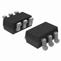
IC INVERTER DUAL TTL HP SOT-363
Manufacturer
ON Semiconductor
Series
7WZr
Datasheet
1.NL27WZ04DFT2G.pdf
(6 pages)
Specifications of NL27WZ04DFT1G
Logic Type
Inverter
Number Of Inputs
1
Number Of Circuits
2
Current - Output High, Low
32mA, 32mA
Voltage - Supply
1.65 V ~ 5.5 V
Operating Temperature
-40°C ~ 85°C
Mounting Type
Surface Mount
Package / Case
SC-70-6, SC-88, SOT-363
Lead Free Status / RoHS Status
Lead free / RoHS Compliant
Available stocks
Company
Part Number
Manufacturer
Quantity
Price
Company:

Part Number:
NL27WZ04DFT1G
Manufacturer:
ON Semiconductor
Quantity:
6
Part Number:
NL27WZ04DFT1G
Manufacturer:
ON/安森美
Quantity:
20 000


Stresses exceeding Maximum Ratings may damage the device. Maximum Ratings are stress ratings only. Functional operation above the
Recommended Operating Conditions is not implied. Extended exposure to stresses above the Recommended Operating Conditions may affect
device reliability.
1. I
2. Measured with minimum pad spacing on an FR4 board, using 10 mm−by−1 inch, 2−ounce copper trace with no air flow.
3. Tested to EIA/JESD22−A114−A
4. Tested to EIA/JESD22−A115−A
5. Tested to JESD22−C101−A
MAXIMUM RATINGS
RECOMMENDED OPERATING CONDITIONS
DC Supply Voltage
DC Input Voltage
DC Output Voltage
DC Input Diode Current
DC Output Diode Current
DC Output Source/Sink Current
DC Supply Current Per Supply Pin
DC Ground Current Per Ground Pin
Storage Temperature Range
Power Dissipation in Still Air
Thermal Resistance
Lead temperature, 1 mm from Case for 10 Seconds
Junction Temperature Under Bias
ESD Withstand Voltage
Supply Voltage
Input Voltage
Output Voltage
Operating Free−Air Temperature
Input Transition Rise or Fall Rate
O
absolute maximum rating must be observed.
Characteristics
Parameter
Output in HIGH or LOW State (Note 1)
Charged Device Model (Note 5)
http://onsemi.com
Human Body Model (Note 3)
SC−88, TSOP−6 (Note 2)
SC−88, TSOP−6 (Note 2)
Machine Model (Note 4)
(HIGH or LOW State)
Data Retention Only
V
2
V
V
CC
CC
CC
= 2.5 V ±0.2 V
=3.0 V ±0.3 V
=5.0 V ±0.5 V
V
Operating
V
O
I
< GND
< GND
Symbol
Symbol
Dt/DV
T
V
I
V
V
I
I
GND
q
V
P
V
T
I
STG
T
T
ESD
V
OK
I
CC
V
CC
IK
CC
O
JA
O
D
O
A
L
J
I
I
1.65
−0.5 ≤ V
Min
−55
−0.5 ≤ V
1.5
0
0
0
0
0
−0.5 to +7.0
−65 to +150
> 2000
Value
> 200
±100
±100
+150
−50
−50
±50
200
333
260
N/A
I
O
≤ +7.0
≤ 7.0
+125
Max
5.5
5.5
5.5
5.5
20
10
5
°C/W
ns/V
Unit
Unit
mW
mA
mA
mA
mA
mA
°C
°C
°C
°C
V
V
V
V
V
V
V
Related parts for NL27WZ04DFT1G
Image
Part Number
Description
Manufacturer
Datasheet
Request
R

Part Number:
Description:
Dual Inverter
Manufacturer:
ON Semiconductor
Datasheet:
Part Number:
Description:
ON Semiconductor [VOLTAGE REGULATOR]
Manufacturer:
ON Semiconductor
Datasheet:
Part Number:
Description:
357-036-542-201 CARDEDGE 36POS DL .156 BLK LOPRO
Manufacturer:
ON Semiconductor
Datasheet:
Part Number:
Description:
357-036-542-201 CARDEDGE 36POS DL .156 BLK LOPRO
Manufacturer:
ON Semiconductor
Datasheet:
Part Number:
Description:
357-036-542-201 CARDEDGE 36POS DL .156 BLK LOPRO
Manufacturer:
ON Semiconductor
Datasheet:
Part Number:
Description:
357-036-542-201 CARDEDGE 36POS DL .156 BLK LOPRO
Manufacturer:
ON Semiconductor
Datasheet:
Part Number:
Description:
357-036-542-201 CARDEDGE 36POS DL .156 BLK LOPRO
Manufacturer:
ON Semiconductor
Datasheet:
Part Number:
Description:
357-036-542-201 CARDEDGE 36POS DL .156 BLK LOPRO
Manufacturer:
ON Semiconductor
Datasheet:
Part Number:
Description:
357-036-542-201 CARDEDGE 36POS DL .156 BLK LOPRO
Manufacturer:
ON Semiconductor
Datasheet:
Part Number:
Description:
357-036-542-201 CARDEDGE 36POS DL .156 BLK LOPRO
Manufacturer:
ON Semiconductor
Datasheet:
Part Number:
Description:
357-036-542-201 CARDEDGE 36POS DL .156 BLK LOPRO
Manufacturer:
ON Semiconductor
Datasheet:
Part Number:
Description:
357-036-542-201 CARDEDGE 36POS DL .156 BLK LOPRO
Manufacturer:
ON Semiconductor
Datasheet:
Part Number:
Description:
Manufacturer:
ON Semiconductor
Datasheet:
Part Number:
Description:
Manufacturer:
ON Semiconductor
Datasheet: