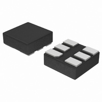
NLX1G332AMX1TCG ON Semiconductor, NLX1G332AMX1TCG Datasheet
NLX1G332AMX1TCG
Specifications of NLX1G332AMX1TCG
Available stocks


Related parts for NLX1G332AMX1TCG

NLX1G332AMX1TCG Summary of contents
Page 1
NLX1G332 3-Input OR Gate The NLX1G332 is an advanced high−speed 3−input CMOS OR gate in ultra−small footprint. The NLX1G332 input structures provide protection when voltages up to 7.0 V are applied, regardless of the supply voltage. Features • High Speed: ...
Page 2
MAXIMUM RATINGS Symbol V DC Supply Voltage Input Voltage Output Voltage OUT I DC Input Diode Current Output Diode Current Output Source/Sink Current Supply Current ...
Page 3
DC ELECTRICAL CHARACTERISTICS Symbol Parameter Conditions V Low−Level IH Input Voltage V Low−Level IL Input Voltage V High− Level I = −100 mA OH Output Voltage ...
Page 4
AC ELECTRICAL CHARACTERISTICS Symbol Parameter t , Propagation Delay, PLH t Input to Output PHL C Input Capacitance IN C Power Dissipation PD Capacitance (Note defined as the value of the internal equivalent capacitance which is ...
Page 5
... Y 50 2.5 ns, 10 MHz Figure 3. Switching Waveforms ORDERING INFORMATION Device NLX1G332AMX1TCG NLX1G332BMX1TCG NLX1G332CMX1TCG †For information on tape and reel specifications, including part orientation and tape sizes, please refer to our Tape and Reel Packaging Specifications Brochure, BRD8011/ INPUT GND t PHL A 1 MHz square input wave is recommended ...
Page 6
... OUTLINE *For additional information on our Pb−Free strategy and soldering C NOTE 3 details, please download the ON Semiconductor Soldering and Mounting Techniques Reference Manual, SOLDERRM/D. http://onsemi.com 6 ASME Y14.5M, 1994. AND IS MEASURED BETWEEN 0.15 AND 0.30 mm FROM THE TERMINAL TIP. PLATED TERMINAL FROM THE EDGE OF THE PACKAGE IS ALLOWED ...
Page 7
... *For additional information on our Pb−Free strategy and soldering NOTE 3 0.05 C details, please download the ON Semiconductor Soldering and Mounting Techniques Reference Manual, SOLDERRM/D. http://onsemi.com 7 1. DIMENSIONING AND TOLERANCING PER ASME Y14.5M, 1994. 2. CONTROLLING DIMENSION: MILLIMETERS. 3. DIMENSION b APPLIES TO PLATED TERMINAL AND IS MEASURED BETWEEN 0.15 AND ...
Page 8
... B *For additional information on our Pb−Free strategy and soldering 0.05 C NOTE 3 details, please download the ON Semiconductor Soldering and Mounting Techniques Reference Manual, SOLDERRM/D. N. American Technical Support: 800−282−9855 Toll Free USA/Canada Europe, Middle East and Africa Technical Support: Phone: 421 33 790 2910 Japan Customer Focus Center Phone: 81− ...