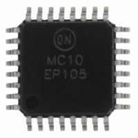
MC10EP105FAR2 ON Semiconductor, MC10EP105FAR2 Datasheet

MC10EP105FAR2
Specifications of MC10EP105FAR2
Available stocks
Related parts for MC10EP105FAR2
MC10EP105FAR2 Summary of contents
Page 1
... Open Input Default State • Safety Clamp on Inputs • Pb−Free Packages are Available* *For additional information on our Pb−Free strategy and soldering details, please download the ON Semiconductor Soldering and Mounting Techniques Reference Manual, SOLDERRM/D. © Semiconductor Components Industries, LLC, 2006 November, 2006 − Rev 3 5 See detailed ordering and shipping information in the package dimensions section on page 9 of this data sheet ...
Page 2
D0b D1a D1a D1b D1b D0b 25 D0a 26 D0a 27 MC10EP105 MC100EP105 ...
Page 3
Table 3. ATTRIBUTES Internal Input Pulldown Resistor Internal Input Pullup Resistor ESD Protection Moisture Sensitivity, Indefinite Time Out of Drypack (Note 1) Flammability Rating Transistor Count Meets or exceeds JEDEC Spec EIA/JESD78 IC Latchup Test 1. For additional information, see ...
Page 4
Table 5. 10EP DC CHARACTERISTICS, PECL Symbol Characteristic I Power Supply Current EE V Output HIGH Voltage (Note Output LOW Voltage (Note Input HIGH Voltage (Single−Ended Input LOW Voltage (Single−Ended ...
Page 5
Table 6. 10EP DC CHARACTERISTICS, PECL Symbol Characteristic I Power Supply Current EE V Output HIGH Voltage (Note Output LOW Voltage (Note Input HIGH Voltage (Single−Ended Input LOW Voltage (Single−Ended ...
Page 6
Table 8. 100EP DC CHARACTERISTICS, PECL Symbol Characteristic I Power Supply Current EE V Output HIGH Voltage (Note 12 Output LOW Voltage (Note 12 Input HIGH Voltage (Single−Ended Input LOW Voltage (Single−Ended ...
Page 7
Table 10. 100EP DC CHARACTERISTICS, NECL Symbol Characteristic I Power Supply Current Output HIGH Voltage (Note 18 Output LOW Voltage (Note 18 Input HIGH Voltage (Single−Ended Input LOW ...
Page 8
FREQUENCY (MHz) Figure 4. F ...
Page 9
... ORDERING INFORMATION Device MC10EP105FA MC10EP105FAG MC10EP105FAR2 MC10EP105FAR2G MC100EP105FA MC100EP105FAG MC100EP105FAR2 MC100EP105FAR2G MC10EP105MNG MC100EP105MNG MC10EP105MNR4G MC100EP105MNR4G †For information on tape and reel specifications, including part orientation and tape sizes, please refer to our Tape and Reel Packaging Specifications Brochure, BRD8011/D. Resource Reference of Application Notes ...
Page 10
−T− DETAIL −Z− −AB− SEATING −AC− PLANE 0.10 (0.004) AC NOTES: 1. DIMENSIONING AND TOLERANCING PER ANSI Y14.5M, 1982. 2. CONTROLLING DIMENSION: MILLIMETER. 3. DATUM PLANE ...
Page 11
... X 0.28 *For additional information on our Pb−Free strategy and soldering details, please download the ON Semiconductor Soldering and Mounting Techniques Reference Manual, SOLDERRM/D. N. American Technical Support: 800−282−9855 Toll Free USA/Canada Europe, Middle East and Africa Technical Support: Phone: 421 33 790 2910 Japan Customer Focus Center Phone: 81− ...


