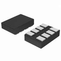
NLX1G99CMX1TCG ON Semiconductor, NLX1G99CMX1TCG Datasheet

NLX1G99CMX1TCG
Specifications of NLX1G99CMX1TCG
Related parts for NLX1G99CMX1TCG
NLX1G99CMX1TCG Summary of contents
Page 1
NLX1G99 Configurable Multifunction Gate The NLX1G99 MiniGatet is an advanced high−speed CMOS multifunction gate with a 3−state output. With the output enable input (OE) at High, the output is disabled and is kept at high impedance. With the output enable ...
Page 2
FUNCTION DIAGRAM FUNCTION TABLE ...
Page 3
Buffer Functions Available Function OE 3−State Buffer L 3−State Inverter Functions Available Function OE 3−State Buffer L 3−State MUX Functions Available Input 1 Input 2 Function 3−State 2−to−1 3−State 2−to−1 3−State 2−to−1, Inverted Out 3−State 2−to−1, Inverted Out LOGIC ...
Page 4
AND/NOR/OR Function Available OE Input 1 Input 2 No. of Inputs AND/NAND Function 2 3−State AND 2 3−State AND OE Input 1 Input 2 No. of Inputs AND/NAND Function 2 3−State AND 2 3−State AND OE Input 1 Input ...
Page 5
NAND/OR Function Available OE Input 1 Input 2 No. of Inputs AND/NAND Function 2 3−State NAND 2 3−State NAND OE Input 1 Input 2 No. of Inputs AND/NAND Function 2 3−State NAND 2 3−State NAND OE Input 1 Input ...
Page 6
XOR/XNOR Function Available Function OE 3−State XOR Function OE 3−State XOR Function OE 3−State XOR Function OE 3−State XNOR 3−State XNOR OE Input 1 Input 2 Figure 13 Input Input 2 H ...
Page 7
MAXIMUM RATINGS Symbol V DC Supply Voltage Input Voltage Output Voltage OUT I DC Input Diode Current Output Diode Current Output Source/Sink Current Supply Current ...
Page 8
DC ELECTRICAL CHARACTERISTICS Symbol Parameter Conditions V Positive T+ Threshold Voltage V Negative T− Threshold Voltage V Hysteresis H Voltage V Minimum T−MIN High−Level V T+MAX Output Voltage I = − ...
Page 9
AC ELECTRICAL CHARACTERISTICS Symbol Parameter V ( Propagation 1.65−1.95 PLH t Delay, Any 2.3 − 2.7 PHL Input to Output 3.0 − 3.6 Y (See Test 4.5 − 5.5 Circuit) t Output Enable 1.65−1.95 EN Time, OE ...
Page 10
TEST CIRCUIT AND VOLTAGE WAVEFORMS From Output R Under Test includes probes and jig capacitance. L Figure 17. Load Circuit 0.2 V ...
Page 11
From Output R Under Test includes probes and jig capacitance. L Figure 22. Load Circuit 0.3 ...
Page 12
... ORDERING INFORMATION Device NLX1G99AMX1TCG NLX1G99BMX1TCG NLX1G99CMX1TCG †For information on tape and reel specifications, including part orientation and tape sizes, please refer to our Tape and Reel Packaging Specifications Brochure, BRD8011/D. Package ULLGA8 − 0.5P (Pb−Free) ULLGA8 − 0.4P (Pb−Free) ULLGA8 − 0.35P (Pb−Free) http://onsemi ...
Page 13
... NOTE 3 0.05 C *For additional information on our Pb−Free strategy and soldering details, please download the ON Semiconductor Soldering and Mounting Techniques Reference Manual, SOLDERRM/D. http://onsemi.com 13 NOTES: 1. DIMENSIONING AND TOLERANCING PER ASME Y14.5M, 1994. 2. CONTROLLING DIMENSION: MILLIMETERS. 3. DIMENSION b APPLIES TO PLATED TERMINAL AND IS MEASURED BETWEEN 0.15 AND ...
Page 14
... 0.05 C NOTE 3 *For additional information on our Pb−Free strategy and soldering details, please download the ON Semiconductor Soldering and Mounting Techniques Reference Manual, SOLDERRM/D. http://onsemi.com 14 NOTES: 1. DIMENSIONING AND TOLERANCING PER ASME Y14.5M, 1994. 2. CONTROLLING DIMENSION: MILLIMETERS. 3. DIMENSION b APPLIES TO PLATED TERMINAL AND IS MEASURED BETWEEN 0.15 AND ...
Page 15
... B 0.05 C NOTE 3 *For additional information on our Pb−Free strategy and soldering details, please download the ON Semiconductor Soldering and Mounting Techniques Reference Manual, SOLDERRM/D. N. American Technical Support: 800−282−9855 Toll Free USA/Canada Europe, Middle East and Africa Technical Support: Phone: 421 33 790 2910 Japan Customer Focus Center Phone: 81− ...


