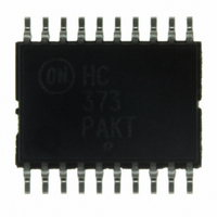
74HC373DTR2G ON Semiconductor, 74HC373DTR2G Datasheet
74HC373DTR2G
Specifications of 74HC373DTR2G
Available stocks


Related parts for 74HC373DTR2G

74HC373DTR2G Summary of contents
Page 1
Octal 3−State Non−Inverting Transparent Latch High−Performance Silicon−Gate CMOS The 74HC373 is identical in pinout to the LS373. The device inputs are compatible with standard CMOS outputs; with pullup resistors, they are compatible with LSTTL outputs. These latches appear transparent ...
Page 2
LOGIC DIAGRAM DATA D3 INPUTS LATCH ENABLE 1 OUTPUT ENABLE Design Criteria Internal Gate Count* Internal Gate Propagation Delay Internal Gate Power Dissipation Speed ...
Page 3
... Input Rise and Fall Time r f (Figure 1) ORDERING INFORMATION Device 74HC373DTR2G †For information on tape and reel specifications, including part orientation and tape sizes, please refer to our Tape and Reel Packaging Specifications Brochure, BRD8011/D. *This package is inherently Pb−Free. Value – 0 7.0 – 0 ...
Page 4
... Maximum Input Leakage Current in I Maximum Three−State OZ Leakage Current I Maximum Quiescent Supply CC Current (per Package) NOTE: Information on typical parametric values can be found in Chapter 2 of the ON Semiconductor High−Speed CMOS Data Book (DL129/D). (Voltages Referenced to GND (V) Test Conditions – 0.1 V 2.0 ...
Page 5
... NOTE: For propagation delays with loads other than 50 pF, and information on typical parametric values, see Chapter 2 of the ON Semiconductor High−Speed CMOS Data Book (DL129/D). C Power Dissipation Capacitance (Per Enabled Output Used to determine the no−load dynamic power consumption Semiconductor High−Speed CMOS Data Book (DL129/D pF, Input 6.0 ns) L ...
Page 6
TIMING REQUIREMENTS ( pF, Input ...
Page 7
TEST POINT OUTPUT DEVICE UNDER TEST *Includes all probe and jig capacitance Figure Figure 7. EXPANDED LOGIC DIAGRAM ...
Page 8
... −V− 0.100 (0.004) −T− SEATING PLANE 16X 0.36 *For additional information on our Pb−Free strategy and soldering details, please download the ON Semiconductor Soldering and Mounting Techniques Reference Manual, SOLDERRM/D. PACKAGE DIMENSIONS TSSOP−20 CASE 948E−02 ISSUE Í Í Í Í ...
Page 9
... Opportunity/Affirmative Action Employer. This literature is subject to all applicable copyright laws and is not for resale in any manner. PUBLICATION ORDERING INFORMATION LITERATURE FULFILLMENT: Literature Distribution Center for ON Semiconductor P.O. Box 5163, Denver, Colorado 80217 USA Phone: 303−675−2175 or 800−344−3860 Toll Free USA/Canada Fax: 303− ...