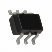
NC7SZ373P6X Fairchild Semiconductor, NC7SZ373P6X Datasheet - Page 3

NC7SZ373P6X
Manufacturer Part Number
NC7SZ373P6X
Description
IC LATCH UHS D 3-STATE SC70-6
Manufacturer
Fairchild Semiconductor
Series
7SZr
Datasheet
1.NC7SZ373P6X.pdf
(9 pages)
Specifications of NC7SZ373P6X
Logic Type
D-Type Transparent Latch
Circuit
1:1
Output Type
Tri-State
Voltage - Supply
1.65 V ~ 5.5 V
Independent Circuits
1
Delay Time - Propagation
2.6ns
Current - Output High, Low
32mA, 32mA
Operating Temperature
-40°C ~ 85°C
Mounting Type
Surface Mount
Package / Case
SC-70-6, SC-88, SOT-363
Number Of Circuits
1
Logic Family
7S
Polarity
Non-Inverting
Input Bias Current (max)
1 uA
High Level Output Current
- 32 mA
Low Level Output Current
32 mA
Propagation Delay Time
5.5 ns at 3.3 V, 4.3 ns at 5 V
Supply Voltage (max)
5.5 V
Supply Voltage (min)
1.65 V
Maximum Operating Temperature
+ 85 C
Minimum Operating Temperature
- 40 C
Mounting Style
SMD/SMT
Lead Free Status / RoHS Status
Lead free / RoHS Compliant
Available stocks
Company
Part Number
Manufacturer
Quantity
Price
Part Number:
NC7SZ373P6X
Manufacturer:
FAIRCHILD/ن»™ç«¥
Quantity:
20 000
V
V
V
V
I
I
I
I
Symbol
IN
OZ
OFF
CC
Absolute Maximum Ratings
DC Electrical Characteristics
IH
IL
OH
OL
Supply Voltage (V
DC Input Voltage (V
DC Output Voltage (V
DC Input Diode Current (I
DC Output Diode Current (I
DC Output (I
DC V
Storage Temperature Range (T
Junction Temperature under Bias (T
Junction Lead Temperature (T
Power Dissipation (P
V
V
(Soldering, 10 seconds)
IN
OUT
CC
HIGH Level Control
Input Voltage
LOW Level Control
Input Voltage
HIGH Level Control
Output Voltage
LOW Level Control
Output Voltage
Input Leakage Current
3-STATE
Output Leakage
Power-Off Leakage Current
Quiescent Supply Current
0V
/GND Current (I
0V
OUT
Parameter
) Source/Sink Current
CC
IN
)
D
)
OUT
) @ 85 C
CC
)
IK
/I
)
OK
GND
)
L
)
STG
)
)
J
1.65 to 1.95 0.75 V
1.65 to 1.95
1.65 to 5.5
1.65 to 5.5
)
2.3 to 5.5
2.3 to 5.5
0 to 5.5
1.65
1.65
1.65
1.65
V
1.8
2.3
3.0
4.5
2.3
3.0
3.0
4.5
1.8
2.3
3.0
4.5
2.3
3.0
3.0
4.5
0.0
(V)
CC
65 C to 150 C
0.5V to 7.0V
0.5V to 7.0V
0.5V to 7.0V
(Note 1)
0.7 V
1.55
1.24
180 mW
Min
1.7
2.2
2.9
4.4
1.9
2.4
2.3
3.8
50 mA
50 mA
50 mA
50 mA
150 C
260 C
CC
CC
T
A
1.65
1.52
2.15
2.68
0.08
0.10
0.15
0.22
0.22
Typ
1.8
2.3
3.0
4.5
2.8
4.2
0.0
0.0
0.0
0.0
0.0
3
25 C
Recommended Operating
Conditions
Note 1: The “Absolute Maximum Ratings”: are those values beyond which
the safety of the device cannot be guaranteed. The device should not be
operated at these limits. The parametric values defined in the Electrical
Characteristics tables are not guaranteed at the absolute maximum ratings.
The “Recommended Operating Conditions” table will define the conditions
for actual device operation.
Note 2: Unused inputs must be held HIGH or LOW. They may not float.
Power Supply
Input Voltage (V
Output Voltage (V
Input Rise and Fall Time (t
Operating Temperature (T
Thermal Resistance (
Operating (V
Data Retention
Active State
3-STATE
V
V
V
1.0
1.0
CC
CC
CC
0.25 V
0.3 V
0.1
0.5
Max
0.08
0.24
0.55
0.55
0.1
0.1
0.1
0.1
0.3
0.4
1.8V, 2.5V
3.3V
5.5V
CC
CC
T
0.75 V
0.7 V
A
CC
1.55
1.29
Min
0.3V
0.5V
IN
1.7
2.2
2.9
4.4
1.9
2.4
2.3
3.8
)
)
OUT
(Note 2)
CC
40 C to 85 C
CC
)
0.2V
JA
0.25 V
0.3 V
)
Max
0.24
0.55
0.55
0.0
0.1
0.1
0.1
0.1
0.3
0.4
A
10
10
1.0
5.0
r
, t
)
CC
f
CC
)
Unit
V
V
V
V
A
A
A
A
www.fairchildsemi.com
V
V
0
V
0
V
V
IN
IN
IN
IN
IN
V
V
or V
IN
OUT
40 C to 85 C
V
V
V
5.5V, GND
Conditions
1.65V to 5.5V
IH
IL
IL
1.5V to 5.5V
OUT
0 to 20 ns/V
0 to 10 ns/V
5.5V
or V
0 to 5 ns/V
0V to 5.5V
0V to 5.5V
I
I
I
I
I
I
I
I
I
I
I
I
0V to V
OH
OH
OH
OH
OH
OH
OL
OL
OL
OL
OL
OL
350 C/W
5.5V
IH
5.5V
100 A
4 mA
8 mA
16 mA
24 mA
32 mA
100 A
4 mA
8 mA
16 mA
24 mA
32 mA
CC


