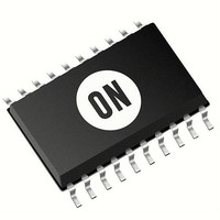
MC74LCX573DTR2G ON Semiconductor, MC74LCX573DTR2G Datasheet - Page 4

MC74LCX573DTR2G
Manufacturer Part Number
MC74LCX573DTR2G
Description
IC LATCH OCT 3ST LV CMOS 20TSSOP
Manufacturer
ON Semiconductor
Series
74LCXr
Type
D-Typer
Datasheet
1.MC74LCX573DTR2G.pdf
(9 pages)
Specifications of MC74LCX573DTR2G
Logic Type
D-Type Transparent Latch
Circuit
8:8
Output Type
Tri-State
Voltage - Supply
2 V ~ 3.6 V
Independent Circuits
1
Delay Time - Propagation
1.5ns
Current - Output High, Low
24mA, 24mA
Operating Temperature
-55°C ~ 125°C
Mounting Type
Surface Mount
Package / Case
20-TSSOP
Logic Family
LCX
Number Of Bits
8
Number Of Elements
1
Latch Mode
Transparent
Polarity
Non-Inverting
Technology
CMOS
Package Type
TSSOP
Propagation Delay Time
10.5ns
Operating Supply Voltage (typ)
2.5/3.3V
High Level Output Current
-24mA
Low Level Output Current
24mA
Operating Supply Voltage (min)
2V
Operating Supply Voltage (max)
3.6V
Operating Temp Range
-55C to 125C
Operating Temperature Classification
Military
Mounting
Surface Mount
Pin Count
20
Number Of Circuits
8
Supply Voltage (max)
3.6 V
Supply Voltage (min)
2 V
Maximum Operating Temperature
+ 85 C
Minimum Operating Temperature
- 40 C
Mounting Style
SMD/SMT
Lead Free Status / RoHS Status
Lead free / RoHS Compliant
Other names
MC74LCX573DTR2GOS
Available stocks
Company
Part Number
Manufacturer
Quantity
Price
Part Number:
MC74LCX573DTR2G
Manufacturer:
ON/安森美
Quantity:
20 000
2. These values of V
3. Skew is defined as the absolute value of the difference between the actual propagation delay for any two separate outputs of the same device.
DC ELECTRICAL CHARACTERISTICS
AC CHARACTERISTICS
V
V
V
V
I
I
I
I
DI
t
t
t
t
t
t
t
t
t
t
t
t
t
Symbol
Symbol
I
OZ
OFF
CC
PLH
PHL
PLH
PHL
PZH
PZL
PHZ
PLZ
s
h
w
OSHL
OSLH
IH
IL
OH
OL
The specification applies to any outputs switching in the same direction, either HIGH-to-LOW (t
guaranteed by design.
CC
HIGH Level Input
Voltage (Note 2)
LOW Level Input
Voltage (Note 2)
HIGH Level Out‐
put Voltage
LOW Level Out‐
put Voltage
Input Leakage
Current
3-State Output
Current
Power-Off Leak‐
age Current
Quiescent Supply
Current
Increase in I
per Input
Propagation Delay
D
Propagation Delay
LE to O
Output Enable Time to HIGH
and LOW Level
Output Disable Time From
High and Low Level
Setup TIme, HIGH or LOW
D
Hold TIme, HIGH or LOW
D
LE Pulse Width, HIGH
Output-to-Output Skew
(Note 3)
Characteristic
n
n
n
to O
to LE
to LE
n
n
I
Parameter
are used to test DC electrical characteristics only.
CC
t
R
= t
2.3 ≤ V
F
2.3 V ≤ V
2.3 ≤ V
2.3 ≤ V
2.3 ≤ V
2.3 V ≤ V
2.3 V ≤ V
= 2.5 ns; R
V
V
V
V
CC
V
V
V
V
CC
CC
CC
CC
V
CC
CC
CC
CC
CC
CC
CC
CC
2.3 V ≤ V
2.7 V ≤ V
2.3 V ≤ V
2.7 V ≤ V
≤ 3.6 V; 3.6 ≤ V
CC
= 0 V; V
= 2.7 V; I
= 3.0 V; I
= 3.0 V; I
Waveform
= 2.3 V; I
= 3.0 V; I
= 3.0 V; I
≤ 3.6 V; V
CC
CC
= 2.7 V; I
≤ 3.6 V; V
≤ 3.6 V; 0V ≤ V
V
= 2.3 V; I
≤ 3.6 V; 0 V ≤ V
I
L
Condition
= V
≤ 3.6 V; I
≤ 3.6 V; I
= 500 W
1
3
2
2
3
3
3
IH
I
CC
CC
CC
CC
or V
OH
OH
OH
OH
OL
OL
or V
OL
IH
OL
I
≤ 2.7 V
≤ 3.6 V
≤ 2.7 V
≤ 3.6 V
= GND or V
= -12 mA
= -18 mA
= -24 mA
= 12 mA
= 16 mA
= 24 mA
= V
http://onsemi.com
= -8 mA
O
OL
OL
= 8 mA
I
V
MC74LCX573
IL
= 5.5 V
or V
CC
= 100 mA
= 100 mA
O
CC
Min
1.5
1.5
1.5
1.5
1.5
1.5
1.5
1.5
2.5
1.5
3.3
≤ 5.5 V;
I
C
= 3.3 V ± 0.3 V
O
≤ 5.5 V
- 0.6 V
L
≤ 5.5 V
= 50 pF
4
CC
Max
8.0
8.0
8.5
8.5
8.5
8.5
6.5
6.5
1.0
1.0
V
T
CC
A
Min
1.7
2.0
1.8
2.2
2.4
2.2
= -40°C to +85°C
T
- 0.2
A
= -55°C to +125°C
Min
1.5
1.5
1.5
1.5
1.5
1.5
1.5
1.5
2.5
1.5
3.3
V
C
CC
L
Limits
= 50 pF
= 2.7 V
Max
0.55
±10
500
0.7
0.8
0.2
0.6
0.4
0.4
±5
±5
10
10
OSHL
Max
9.0
9.0
9.5
9.5
9.5
9.5
7.0
7.0
) or LOW-to-HIGH (t
V
T
A
CC
V
Min
1.7
2.0
1.8
2.2
2.4
2.2
= -55°C to +125°C
CC
- 0.2
Min
1.5
1.5
1.5
1.5
1.5
1.5
1.5
1.5
4.0
2.0
4.0
C
= 2.5 V ± 0.2 V
L
= 30 pF
Max
0.60
±10
500
0.7
0.8
0.2
0.6
0.4
0.4
Max
10.5
10.5
10.5
10.5
±5
±5
10
10
9.6
9.6
7.8
7.8
OSLH
); parameter
Unit
Unit
mA
mA
mA
mA
mA
ns
ns
ns
ns
ns
V
V
V
V


