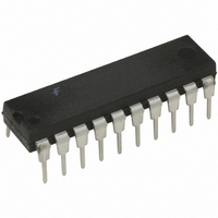
74F533PC Fairchild Semiconductor, 74F533PC Datasheet - Page 2

74F533PC
Manufacturer Part Number
74F533PC
Description
IC LATCH TRANSP OCT 3ST 20-DIP
Manufacturer
Fairchild Semiconductor
Series
74Fr
Datasheet
1.74F533PC.pdf
(7 pages)
Specifications of 74F533PC
Logic Type
D-Type Transparent Latch
Circuit
8:8
Output Type
Tri-State
Voltage - Supply
4.5 V ~ 5.5 V
Independent Circuits
1
Delay Time - Propagation
6.7ns
Current - Output High, Low
3mA, 24mA
Operating Temperature
0°C ~ 70°C
Mounting Type
Through Hole
Package / Case
20-DIP (0.300", 7.62mm)
Lead Free Status / RoHS Status
Lead free / RoHS Compliant
Other names
74F533
www.fairchildsemi.com
Unit Loading/Fan Out
Function Table
H
L
X
Logic Diagram
Please note that this diagram is provided only for the understanding of logic operations and should not be used to estimate propagation delays.
LOW Voltage Level
HIGH Voltage Level
Immaterial
D
LE
OE
O
0
0
LE
Pin Names
H
H
X
–D
–O
L
7
7
Inputs
OE
H
L
L
L
Data Inputs
Latch Enable Input (Active HIGH)
Output Enable Input (Active LOW)
Complementary 3-STATE Outputs
D
H
X
X
L
Description
Output
O
O
H
Z
L
0
2
Functional Description
The 74F533 contains eight D-type latches with 3-STATE
output buffers. When the Latch Enable (LE) input is HIGH,
data on the D
the latches are transparent, i.e., a latch output will change
state each time its D input changes. When LE is LOW, the
latches store the information that was present on the D
inputs a setup time preceding the HIGH-to-LOW transition
of LE. The 3-STATE buffers are controlled by the Output
Enable (OE) input. When OE is LOW, the buffers are in the
bi-state mode. When OE is HIGH the buffers are in the high
impedance mode but this does not interfere with entering
new data into the latches.
150/40 (33.3)
HIGH/LOW
1.0/1.0
1.0/1.0
1.0/1.0
U.L.
n
inputs enters the latches. In this condition
3 mA/24 mA (20 mA)
Output I
20 A/ 0.6 mA
20 A/ 0.6 mA
20 A/ 0.6 mA
Input I
IH
OH
/I
/I
IL
OL


